• Photonics Research
  • Vol. 5, Issue 2, 108 (2017)
Huanying Zhou1, Ciyuan Qiu1、3、*, Xinhong Jiang1, Qingming Zhu1, Yu He1, Yong Zhang1, Yikai Su1、4、*, and Richard Soref2
Author Affiliations
  • 1State Key Lab of Advanced Optical Communication Systems and Networks, Department of Electronic Engineering, Shanghai Jiao Tong University, Shanghai 200240, China
  • 2Engineering Department, University of Massachusetts, Boston, Massachusetts 02125, USA
  • 3e-mail: qiuciyuan@sjtu.edu.cn
  • 4e-mail: yikaisu@sjtu.edu.cn
  • show less
    DOI: 10.1364/PRJ.5.000108 Cite this Article Set citation alerts
    Huanying Zhou, Ciyuan Qiu, Xinhong Jiang, Qingming Zhu, Yu He, Yong Zhang, Yikai Su, Richard Soref. Compact, submilliwatt, 2 × 2 silicon thermo-optic switch based on photonic crystal nanobeam cavities[J]. Photonics Research, 2017, 5(2): 108 Copy Citation Text show less
    (a) Schematic diagram of the proposed 2×2 TO switch based on dual PCN cavities. The phase difference between the two arms (Φ1−Φ2) is equal to π. (b) Cross-section view of the coupled region in one half of the proposed 2×2 TO switch.
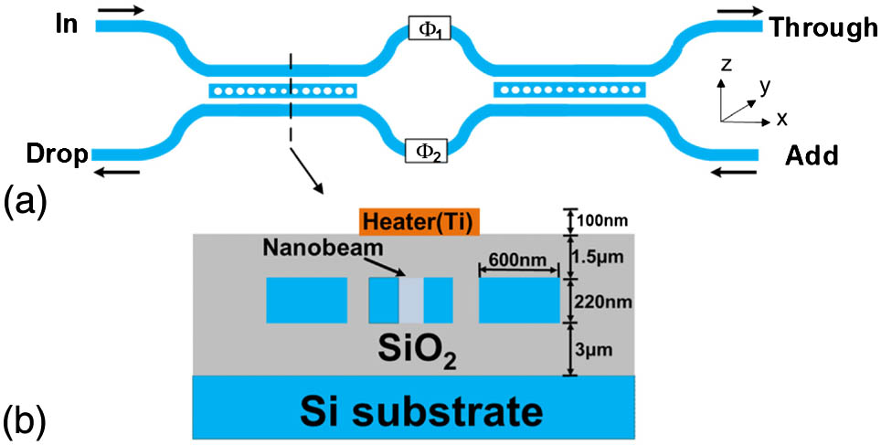
    Fig. 1. (a) Schematic diagram of the proposed 2×2 TO switch based on dual PCN cavities. The phase difference between the two arms (Φ1Φ2) is equal to π. (b) Cross-section view of the coupled region in one half of the proposed 2×2 TO switch.
    (a) Calculated electric field distribution of a single PCN 3W structure at the resonant wavelength based on 2.5D variational FDTD simulation. (b) Simulated transmission spectra of a single PCN 3W structure.
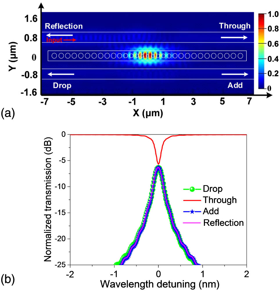
    Fig. 2. (a) Calculated electric field distribution of a single PCN 3W structure at the resonant wavelength based on 2.5D variational FDTD simulation. (b) Simulated transmission spectra of a single PCN 3W structure.
    (a) Micrograph of the fabricated 2×2 TO switch based on dual PCN 3W structures. (b) SEM image of the fabricated PCN 3W structure. (c) Device after wire bonding to a PCB.
    Fig. 3. (a) Micrograph of the fabricated 2×2 TO switch based on dual PCN 3W structures. (b) SEM image of the fabricated PCN 3W structure. (c) Device after wire bonding to a PCB.
    Transmission spectra of a fabricated single PCN 3W structure in through (red solid), drop (green solid), and add (blue dash) ports. Note that the transmissions are normalized to a reference waveguide and the same to the below measured transmission spectra.
    Fig. 4. Transmission spectra of a fabricated single PCN 3W structure in through (red solid), drop (green solid), and add (blue dash) ports. Note that the transmissions are normalized to a reference waveguide and the same to the below measured transmission spectra.
    (a) Transmission spectra of the fabricated 2×2 TO switch based on dual PCN 3W structures with the unaligned wavelength state (solid lines) and the aligned wavelength state (lines with symbols). (b) Transmission spectra of the fabricated 2×2 TO switch based on dual PCN 3W structures with a π phase difference at through (red line)/drop (blue line)/add (green line) ports.
    Fig. 5. (a) Transmission spectra of the fabricated 2×2 TO switch based on dual PCN 3W structures with the unaligned wavelength state (solid lines) and the aligned wavelength state (lines with symbols). (b) Transmission spectra of the fabricated 2×2 TO switch based on dual PCN 3W structures with a π phase difference at through (red line)/drop (blue line)/add (green line) ports.
    (a) Transmission spectra of the fabricated 2×2 TO switch based on dual PCN 3W structures with various applied powers (P1,P2,P3) at the through ports (solid lines) and the drop ports (lines with symbols). (b) Fitting curve of the resonance wavelength shift of 2×2 TO switch based on dual PCN 3W structures as a function of the applied power.
    Fig. 6. (a) Transmission spectra of the fabricated 2×2 TO switch based on dual PCN 3W structures with various applied powers (P1,P2,P3) at the through ports (solid lines) and the drop ports (lines with symbols). (b) Fitting curve of the resonance wavelength shift of 2×2 TO switch based on dual PCN 3W structures as a function of the applied power.
    TypesDevice FootprintThermal Tuning EfficiencySwitching Power
    Adiabatic bend-based MZI [28]5000  μm212.7 mW
    MRR [29]400  μm20.25 nm/mW3.3 mW
    MZI [30]>10000  μm230 mW
    Dual MRRs [31]1000  μm20.9 nm/mW6.8 mW
    Photonic crystal [32]35  μm×10  μm0.63 nm/mW18.2 mW
    2D waveguide-based MZI [33]42  μm×42  μm26 mW
    Our work30  μm×150  μm1.23 nm/mW0.16 mW
    Table 1. Comparisons of the Operation Performances of Various Silicon TO Switches
    Huanying Zhou, Ciyuan Qiu, Xinhong Jiang, Qingming Zhu, Yu He, Yong Zhang, Yikai Su, Richard Soref. Compact, submilliwatt, 2 × 2 silicon thermo-optic switch based on photonic crystal nanobeam cavities[J]. Photonics Research, 2017, 5(2): 108
    Download Citation