• Photonics Research
  • Vol. 11, Issue 2, 252 (2023)
Anna Fedotova1、2、*, Mohammadreza Younesi2, Maximilian Weissflog2、3, Dennis Arslan1、2, Thomas Pertsch2、3、4, Isabelle Staude1、2、3, and Frank Setzpfandt2、4
Author Affiliations
  • 1Institute of Solid State Physics, Friedrich Schiller University Jena, 07743 Jena, Germany
  • 2Institute of Applied Physics, Abbe Center of Photonics, Friedrich Schiller University Jena, 07745 Jena, Germany
  • 3Max Planck School of Photonics, 07745 Jena, Germany
  • 4Fraunhofer Institute for Applied Optics and Precision Engineering, 07745 Jena, Germany
  • show less
    DOI: 10.1364/PRJ.475616 Cite this Article Set citation alerts
    Anna Fedotova, Mohammadreza Younesi, Maximilian Weissflog, Dennis Arslan, Thomas Pertsch, Isabelle Staude, Frank Setzpfandt. Spatially engineered nonlinearity in resonant metasurfaces[J]. Photonics Research, 2023, 11(2): 252 Copy Citation Text show less
    (a) SEM image of an example metasurface. The false red color shows regions with altered by electric field poling second-order nonlinear susceptibility χ(2). The false blue color marks the regions where χ(2) was not affected. d is the period of nanostructuring (or the geometric diffraction grating), and p is the period of grating formed by alternating signs of χ(2) (or the new nonlinear grating). (b) Scheme of the k-space (diffraction pattern) of such a metasurface as in (a) for SH. The blue orders appear from the nanostructure grating and the green ones from the additional nonlinear grating. In the experiment, we collected only the orders propagating under angles accepted by the NA of our collection objective (marked as a gray circle). (c) Polarization-contrast microscopy image of a poled LN thin film. Dark areas on the top and bottom are electrodes, and triangle areas in the middle are poled regions. False colors mark poled and nonpoled parts. The poling period here is p=3 μm. (d) and (e) Experimental transmittance spectra of three metasurfaces with the same geometric parameters (left y-axis): poled metasurface (red), nonpoled metasurface (blue), and large nonpoled metasurface (pink) for polarization along the LN optic axis (d) and perpendicular to it (e). Dotted curves show simulated transmittance for an infinite metasurface (right y-axis). (f) and (g) Enhancement of the electric field inside a nanoresonator at two wavelengths: (f) electric dipole (ED) resonance, and (g) magnetic dipole (MD) resonance.
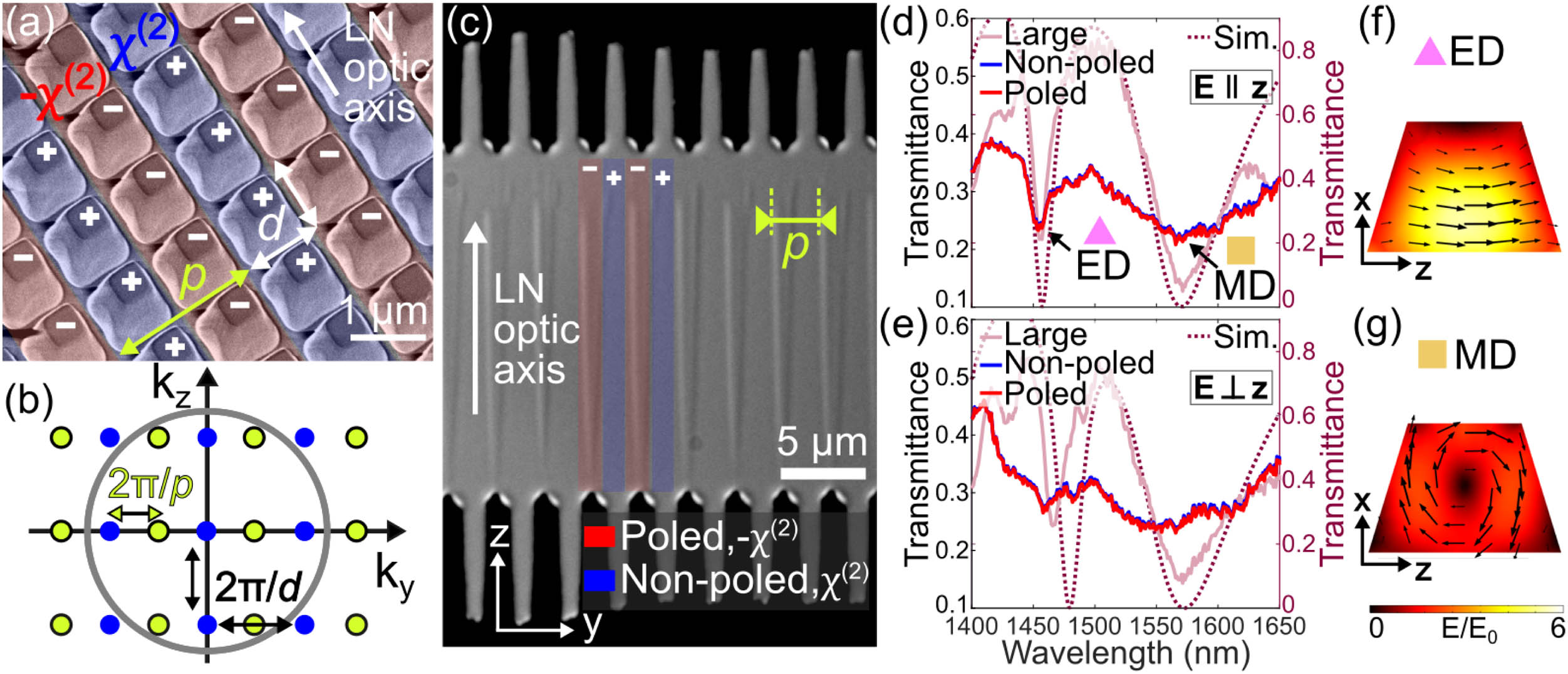
    Fig. 1. (a) SEM image of an example metasurface. The false red color shows regions with altered by electric field poling second-order nonlinear susceptibility χ(2). The false blue color marks the regions where χ(2) was not affected. d is the period of nanostructuring (or the geometric diffraction grating), and p is the period of grating formed by alternating signs of χ(2) (or the new nonlinear grating). (b) Scheme of the k-space (diffraction pattern) of such a metasurface as in (a) for SH. The blue orders appear from the nanostructure grating and the green ones from the additional nonlinear grating. In the experiment, we collected only the orders propagating under angles accepted by the NA of our collection objective (marked as a gray circle). (c) Polarization-contrast microscopy image of a poled LN thin film. Dark areas on the top and bottom are electrodes, and triangle areas in the middle are poled regions. False colors mark poled and nonpoled parts. The poling period here is p=3  μm. (d) and (e) Experimental transmittance spectra of three metasurfaces with the same geometric parameters (left y-axis): poled metasurface (red), nonpoled metasurface (blue), and large nonpoled metasurface (pink) for polarization along the LN optic axis (d) and perpendicular to it (e). Dotted curves show simulated transmittance for an infinite metasurface (right y-axis). (f) and (g) Enhancement of the electric field inside a nanoresonator at two wavelengths: (f) electric dipole (ED) resonance, and (g) magnetic dipole (MD) resonance.
    (a)–(h) Experimental real-space images of the second harmonic from various metasurfaces. The top row contains the poled metasurfaces and shows an exemplary scheme of χ(2)-distributions, and the bottom row contains the nonpoled metasurfaces. (a) Poled 1D metasurface (nanograting) with structure period d=1.2 μm and ridge width 0.6 μm, poling period p=2 μm, excited with the nonresonant pump wavelength ∼1550 nm. (e) Corresponding nonpoled 1D metasurface (nanograting) with the same d and ridge width. (b) and (c) poled 2D metasurfaces with structure period d=1 μm, poling period p=2 μm, excited with the nonresonant pump wavelength 1412 nm. In (b), the nanoresonators are supposed to be either completely poled (−χ(2)) or completely nonpoled (χ(2)). In (c), the domain border is supposed to be inside a nanoresonator based on the relative positioning of the fabricated nanoresonator array with respect to the poled regions of the thin film. (d) Poled 2D metasurface with the same geometric parameters as in (b) and (c), but the poling period is p=3 μm. (f)–(h) Nonpoled metasurfaces with the same d=1 μm and geometry of the nanoresonators. Each image is normalized to its maximum SHG value, and the pump polarization is oriented along the LN optic axis, which is shown as a white arrow. (i) Integrated SHG signal from metasurfaces in (a)–(h). The values extracted from (a) and (e) are multiplied by 10. SHG is normalized to the value from (d), and the error bars account for a pump power variation of 10%.
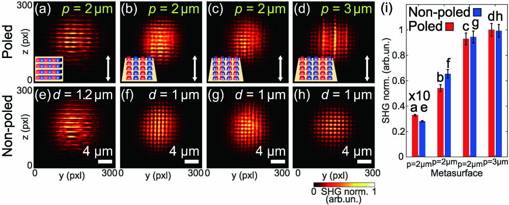
    Fig. 2. (a)–(h) Experimental real-space images of the second harmonic from various metasurfaces. The top row contains the poled metasurfaces and shows an exemplary scheme of χ(2)-distributions, and the bottom row contains the nonpoled metasurfaces. (a) Poled 1D metasurface (nanograting) with structure period d=1.2  μm and ridge width 0.6 μm, poling period p=2  μm, excited with the nonresonant pump wavelength 1550  nm. (e) Corresponding nonpoled 1D metasurface (nanograting) with the same d and ridge width. (b) and (c) poled 2D metasurfaces with structure period d=1  μm, poling period p=2  μm, excited with the nonresonant pump wavelength 1412 nm. In (b), the nanoresonators are supposed to be either completely poled (χ(2)) or completely nonpoled (χ(2)). In (c), the domain border is supposed to be inside a nanoresonator based on the relative positioning of the fabricated nanoresonator array with respect to the poled regions of the thin film. (d) Poled 2D metasurface with the same geometric parameters as in (b) and (c), but the poling period is p=3  μm. (f)–(h) Nonpoled metasurfaces with the same d=1  μm and geometry of the nanoresonators. Each image is normalized to its maximum SHG value, and the pump polarization is oriented along the LN optic axis, which is shown as a white arrow. (i) Integrated SHG signal from metasurfaces in (a)–(h). The values extracted from (a) and (e) are multiplied by 10. SHG is normalized to the value from (d), and the error bars account for a pump power variation of 10%.
    (a), (b) Sketches of 1D poled metasurfaces and (c)–(f) experimental images of SH diffraction patterns of 1D poled metasurfaces with LN ridges (c) along y-axis and (d) rotated by 60°, as well as nonpoled reference metasurfaces, (e) and (f), correspondingly. The poling period is p=2 μm, the nanograting period is d=1.2 μm, and the ridge width is 0.6 μm. The pump wavelength is ∼1550 nm, and the polarization is along the LN optic axis. The vertical lines coming through the 0th and 1st geometric orders are associated with the blooming effect of the EMCCD camera. The SHG in each image (c)–(f) is normalized to its maximum value. kp marks the nonlinear grating wavevector. (g)–(i) Analytical and (j)–(l) experimental images of SH diffraction patterns of 2D poled metasurfaces with poling periods (g) and (j) p=2 μm, (h) and (k) 3 μm, and (i) and (l) 4 μm. (m)–(o) Corresponding nonpoled metasurfaces. The blue dots mark the geometric diffraction orders, and the green dots mark nonlinear χ(2)-orders. The gray circles in (g)–(i) correspond to the NA of our collecting objective. The pump wavelength is 1412 nm, and polarization is along the LN optic axis. SHG in each image (j)–(o) is normalized to its maximum value and plotted on a logarithmic scale. The green circles in all subfigures mark the diffraction orders associated with the χ(2)-grating.
    Fig. 3. (a), (b) Sketches of 1D poled metasurfaces and (c)–(f) experimental images of SH diffraction patterns of 1D poled metasurfaces with LN ridges (c) along y-axis and (d) rotated by 60°, as well as nonpoled reference metasurfaces, (e) and (f), correspondingly. The poling period is p=2  μm, the nanograting period is d=1.2  μm, and the ridge width is 0.6 μm. The pump wavelength is 1550  nm, and the polarization is along the LN optic axis. The vertical lines coming through the 0th and 1st geometric orders are associated with the blooming effect of the EMCCD camera. The SHG in each image (c)–(f) is normalized to its maximum value. kp marks the nonlinear grating wavevector. (g)–(i) Analytical and (j)–(l) experimental images of SH diffraction patterns of 2D poled metasurfaces with poling periods (g) and (j) p=2  μm, (h) and (k) 3 μm, and (i) and (l) 4 μm. (m)–(o) Corresponding nonpoled metasurfaces. The blue dots mark the geometric diffraction orders, and the green dots mark nonlinear χ(2)-orders. The gray circles in (g)–(i) correspond to the NA of our collecting objective. The pump wavelength is 1412 nm, and polarization is along the LN optic axis. SHG in each image (j)–(o) is normalized to its maximum value and plotted on a logarithmic scale. The green circles in all subfigures mark the diffraction orders associated with the χ(2)-grating.
    (a)–(f) Experimental images of the SH diffraction pattern from poled (top row) with poling period p=2 μm and nonpoled (bottom row) metasurfaces for different pump wavelengths: (a) and (d) pump 1412 nm, nonresonant case, (b) and (e) pump 1456 nm, electric dipole resonance, (c) and (f) pump 1565 nm, magnetic dipole resonance. Polarization is along the optic axis. Geometric orders are indicated by blue circles, and nonlinear orders are indicated by green circles. Dash-dotted rectangles mark the orders used in (g) and (i). SHG is normalized to the maximum value in each plot. (g) Experimental and (h) simulated SHG signals for the orders from the central row (n, 0), where n={±1,±1p,0} for poled metasurfaces in (a)–(c). Similarly, (i) experimental and (j) simulated SHG signals for the orders from the central row for nonpoled metasurfaces in (d)–(f). Geometric orders are indicated as 0 and ±1, and nonlinear orders are indicated as ±1p. The SHG signal in each order was calculated by integration inside corresponding blue (linear) or green (nonlinear) circles. In (g) and (i) SHG values are normalized to the value of (0,0) for ED for each respective case. The LN substrate thickness in the simulations is 750 nm.
    Fig. 4. (a)–(f) Experimental images of the SH diffraction pattern from poled (top row) with poling period p=2  μm and nonpoled (bottom row) metasurfaces for different pump wavelengths: (a) and (d) pump 1412 nm, nonresonant case, (b) and (e) pump 1456 nm, electric dipole resonance, (c) and (f) pump 1565 nm, magnetic dipole resonance. Polarization is along the optic axis. Geometric orders are indicated by blue circles, and nonlinear orders are indicated by green circles. Dash-dotted rectangles mark the orders used in (g) and (i). SHG is normalized to the maximum value in each plot. (g) Experimental and (h) simulated SHG signals for the orders from the central row (n, 0), where n={±1,±1p,0} for poled metasurfaces in (a)–(c). Similarly, (i) experimental and (j) simulated SHG signals for the orders from the central row for nonpoled metasurfaces in (d)–(f). Geometric orders are indicated as 0 and ±1, and nonlinear orders are indicated as ±1p. The SHG signal in each order was calculated by integration inside corresponding blue (linear) or green (nonlinear) circles. In (g) and (i) SHG values are normalized to the value of (0,0) for ED for each respective case. The LN substrate thickness in the simulations is 750 nm.
    (a)–(c) SHG diffraction patterns for the metasurface with poling period p=3 μm for the pump wavelengths: (a) nonresonant, at the (b) ED resonance and (c) MD resonance. The orders (0,0), (±1, 0), and (0, ±1) are the geometric orders and are marked blue. The orders (±1p, 0), (±2p, 0), and (0, ±1p) are χ(2)-orders and are marked green. The white and black arrows show the polarization direction along the LN optic axis. The SHG is normalized to the maximum value. (d)–(f) The SHG for different pump polarizations in (±2p, 0) and (g)–(i) in (±1p, 0) orders. The values are normalized to the maximum value in each plot. Gray circles/triangles/squares show the background.
    Fig. 5. (a)–(c) SHG diffraction patterns for the metasurface with poling period p=3  μm for the pump wavelengths: (a) nonresonant, at the (b) ED resonance and (c) MD resonance. The orders (0,0), (±1, 0), and (0, ±1) are the geometric orders and are marked blue. The orders (±1p, 0), (±2p, 0), and (0, ±1p) are χ(2)-orders and are marked green. The white and black arrows show the polarization direction along the LN optic axis. The SHG is normalized to the maximum value. (d)–(f) The SHG for different pump polarizations in (±2p, 0) and (g)–(i) in (±1p, 0) orders. The values are normalized to the maximum value in each plot. Gray circles/triangles/squares show the background.
    Anna Fedotova, Mohammadreza Younesi, Maximilian Weissflog, Dennis Arslan, Thomas Pertsch, Isabelle Staude, Frank Setzpfandt. Spatially engineered nonlinearity in resonant metasurfaces[J]. Photonics Research, 2023, 11(2): 252
    Download Citation