• Photonics Research
  • Vol. 8, Issue 10, 1634 (2020)
Jinfeng Mu*, Meindert Dijkstra, Jeroen Korterik, Herman Offerhaus, and Sonia M. García-Blanco
Author Affiliations
  • Optical Sciences Group, MESA+ Institute for Nanotechnology, University of Twente, 7500 AE Enschede, The Netherlands
  • show less
    DOI: 10.1364/PRJ.401055 Cite this Article Set citation alerts
    Jinfeng Mu, Meindert Dijkstra, Jeroen Korterik, Herman Offerhaus, Sonia M. García-Blanco, "High-gain waveguide amplifiers in Si3N4 technology via double-layer monolithic integration," Photonics Res. 8, 1634 (2020) Copy Citation Text show less
    Structure of the monolithically integrated Al2O3:Er3+-Si3N4 amplifier. (a) 3D schematic of the whole amplifier chip with MMI-based multi/demultiplexer. P and S indicate the pump port and the signal port of the MMI multi/demultiplexer, respectively. (b) Schematic of the adiabatic vertical coupler, consisting of a vertical Si3N4 taper and a lateral Al2O3:Er3+ taper. (c) Cross sections of the adiabatic coupler at different positions (A, B, C, D, E) indicated in (b) within the taper region along the propagation direction, and the related mode intensity profiles under transverse electric (TE) polarization. The different cross-sectional parameters are indicated. The field intensity is visualized in the rainbow color scale, where the highest intensity is represented by the red.
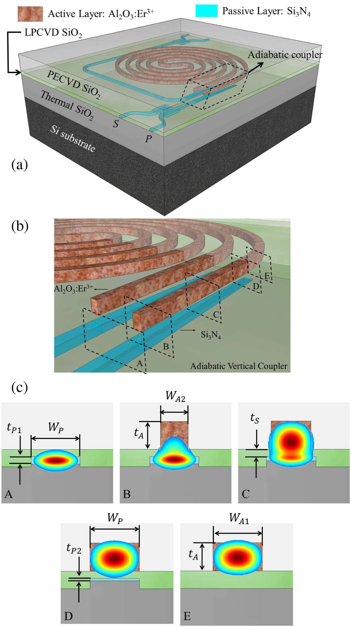
    Fig. 1. Structure of the monolithically integrated Al2O3:Er3+-Si3N4 amplifier. (a) 3D schematic of the whole amplifier chip with MMI-based multi/demultiplexer. P and S indicate the pump port and the signal port of the MMI multi/demultiplexer, respectively. (b) Schematic of the adiabatic vertical coupler, consisting of a vertical Si3N4 taper and a lateral Al2O3:Er3+ taper. (c) Cross sections of the adiabatic coupler at different positions (A, B, C, D, E) indicated in (b) within the taper region along the propagation direction, and the related mode intensity profiles under transverse electric (TE) polarization. The different cross-sectional parameters are indicated. The field intensity is visualized in the rainbow color scale, where the highest intensity is represented by the red.
    SEM images of the cross sections (a) nearby the tip of the Al2O3 taper and (b) nearby the tip of the Si3N4 taper. The SEM images were captured from a cleaved sample from a monitor wafer with undoped Al2O3 on the Si3N4 platform.
    Fig. 2. SEM images of the cross sections (a) nearby the tip of the Al2O3 taper and (b) nearby the tip of the Si3N4 taper. The SEM images were captured from a cleaved sample from a monitor wafer with undoped Al2O3 on the Si3N4 platform.
    Characterization of losses. (a) Measured intensity of the light scattered along the length of the Al2O3:Er3+ waveguide spirals at different wavelengths. Launched signal power is −30 dBm. (b) Measured absorption plus propagation losses of the Al2O3:Er3+ waveguide spiral as a function of launched signal power.
    Fig. 3. Characterization of losses. (a) Measured intensity of the light scattered along the length of the Al2O3:Er3+ waveguide spirals at different wavelengths. Launched signal power is 30  dBm. (b) Measured absorption plus propagation losses of the Al2O3:Er3+ waveguide spiral as a function of launched signal power.
    (a) Measured absorption plus propagation losses as a function wavelength for a launched signal power of −30 dBm. The red line shows the calculated values from the absorption cross sections presented in the work of Ref. [41] for an ion concentration of 1.65×1020 cm−3. (b) Transmitted power as a function of the number of Al2O3:Er3+-Si3N4 adiabatic couplers at the wavelength of 1306 nm. A loss per coupler of 0.49 dB was obtained. (c) Si3N4 multi/demultiplexer loss spectra by launching through the pump and signal ports at the wavelength of 1460–1635 nm. The shadows indicate the standard deviation of the measurement.
    Fig. 4. (a) Measured absorption plus propagation losses as a function wavelength for a launched signal power of 30  dBm. The red line shows the calculated values from the absorption cross sections presented in the work of Ref. [41] for an ion concentration of 1.65×10²⁰  cm3. (b) Transmitted power as a function of the number of Al2O3:Er3+-Si3N4 adiabatic couplers at the wavelength of 1306 nm. A loss per coupler of 0.49 dB was obtained. (c) Si3N4 multi/demultiplexer loss spectra by launching through the pump and signal ports at the wavelength of 1460–1635 nm. The shadows indicate the standard deviation of the measurement.
    Experimental setup utilized for the measurement of the net gain on the Al2O3:Er3+-Si3N4 integrated spiral amplifier. The pump light, at 976.2 nm, is split by a 3 dB coupler (operating wavelength 980 nm) and injected into the amplifier chip from both the input and output sides via MMI multi/demultiplexers. The signal, from a tunable laser operating in the C-band, is injected from the left and collected on the right side and directed to the optical spectrum analyzer. The photographs represent the integrated spiral amplifier in the pump-on and pump-off cases. The pitch between adjacent loops of the Al2O3:Er3+ spiral is 40 μm.
    Fig. 5. Experimental setup utilized for the measurement of the net gain on the Al2O3:Er3+-Si3N4 integrated spiral amplifier. The pump light, at 976.2 nm, is split by a 3 dB coupler (operating wavelength 980 nm) and injected into the amplifier chip from both the input and output sides via MMI multi/demultiplexers. The signal, from a tunable laser operating in the C-band, is injected from the left and collected on the right side and directed to the optical spectrum analyzer. The photographs represent the integrated spiral amplifier in the pump-on and pump-off cases. The pitch between adjacent loops of the Al2O3:Er3+ spiral is 40 μm.
    Measured spectra from the OSA at the wavelength of 1550 nm under (a) pump-off case and (b) pump-on case. The legend indicates the launched signal powers. The launched pump power is ∼50 mW.
    Fig. 6. Measured spectra from the OSA at the wavelength of 1550 nm under (a) pump-off case and (b) pump-on case. The legend indicates the launched signal powers. The launched pump power is 50  mW.
    Net gain measurements. (a) Net gain of the integrated amplifier as a function of launched pump power for different launched signal powers (1532 nm of wavelength). (b) Net gain as a function of launched signal power for three different wavelengths within the C-band. The launched pump power is 50 mW. The dashed lines indicate 3 dB drop from the maximum gains for the three wavelengths. (c) Net gain as a function of wavelength for a launched signal power of 30 dBm and launched pump power of 50 mW. A bidirectional pumping scheme is applied. The reported launched power corresponds to the sum of the powers launched in each of the two input ports.
    Fig. 7. Net gain measurements. (a) Net gain of the integrated amplifier as a function of launched pump power for different launched signal powers (1532 nm of wavelength). (b) Net gain as a function of launched signal power for three different wavelengths within the C-band. The launched pump power is 50 mW. The dashed lines indicate 3 dB drop from the maximum gains for the three wavelengths. (c) Net gain as a function of wavelength for a launched signal power of 30 dBm and launched pump power of 50 mW. A bidirectional pumping scheme is applied. The reported launched power corresponds to the sum of the powers launched in each of the two input ports.
    Jinfeng Mu, Meindert Dijkstra, Jeroen Korterik, Herman Offerhaus, Sonia M. García-Blanco, "High-gain waveguide amplifiers in Si3N4 technology via double-layer monolithic integration," Photonics Res. 8, 1634 (2020)
    Download Citation