• Acta Optica Sinica
  • Vol. 41, Issue 7, 0716001 (2021)
Shiguang Shang1、*, Lang Gao1、**, Wei Ren2, Wenqian Zhang1, and Rui Wang1
Author Affiliations
  • 1College of Electronic Engineering, Xi′an University of Posts and Telecommunications, Xi′an, Shaanxi 710121, China
  • 2College of Science, Xi′an University of Posts and Telecommunications, Xi′an, Shaanxi 710121, China
  • show less
    DOI: 10.3788/AOS202141.0716001 Cite this Article Set citation alerts
    Shiguang Shang, Lang Gao, Wei Ren, Wenqian Zhang, Rui Wang. Fabrication of ZnO Nanowalls by Electrochemical Deposition and Ultraviolet Detection Performance[J]. Acta Optica Sinica, 2021, 41(7): 0716001 Copy Citation Text show less
    Schematic of electrode. (a) Top view of electrode; (b) schematic of electrode layered structure
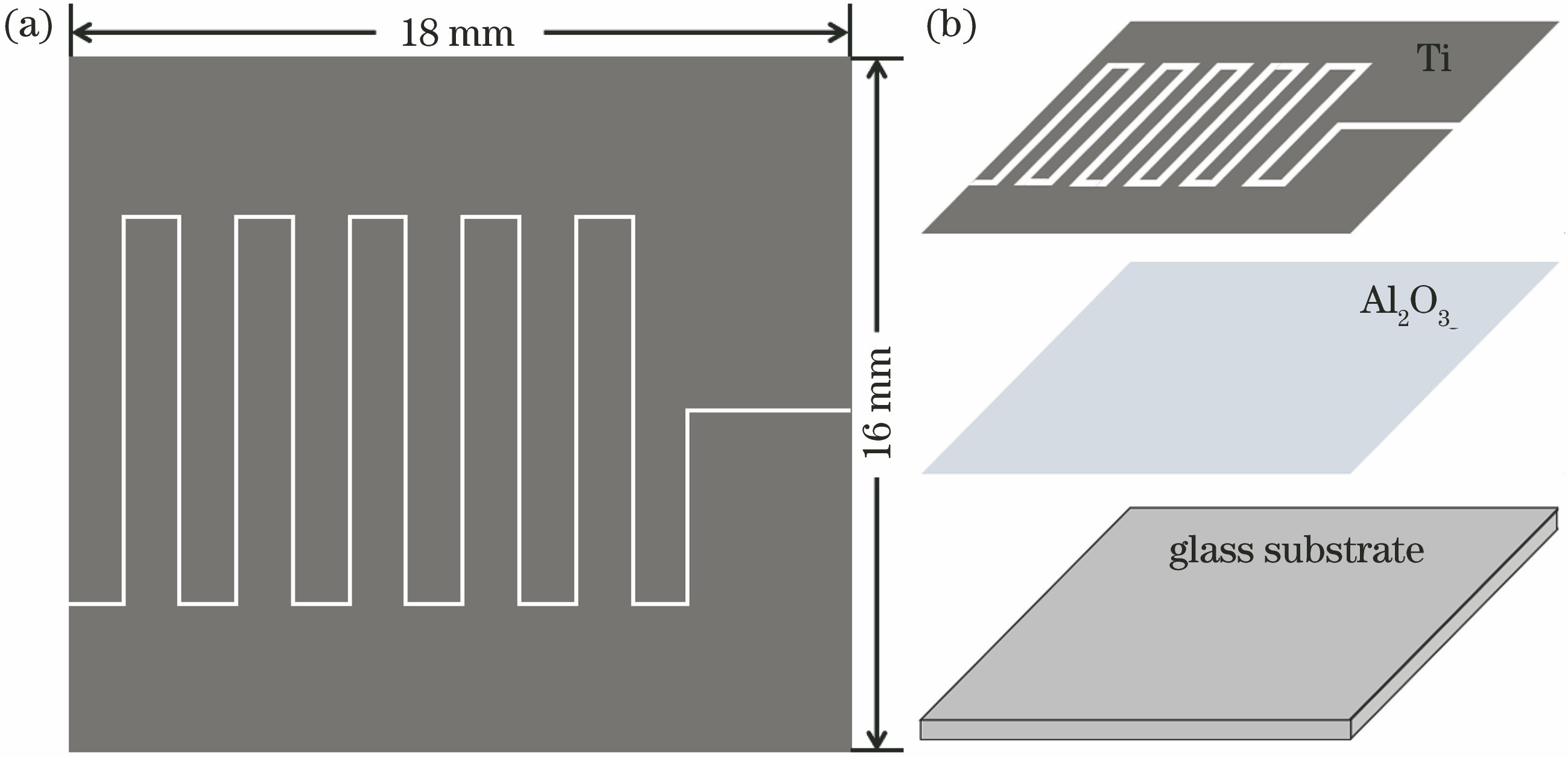
    Fig. 1. Schematic of electrode. (a) Top view of electrode; (b) schematic of electrode layered structure
    SEM images of ZnO nanowalls grown at different deposition voltages and EDS spectrum of ZnO nanowalls grown at deposition voltage of 1.6 V. (a) 1.4 V; (b) 1.6 V; (c) 1.8 V; (d) 2.0 V; (e) 2.2 V; (f) EDS spectrum
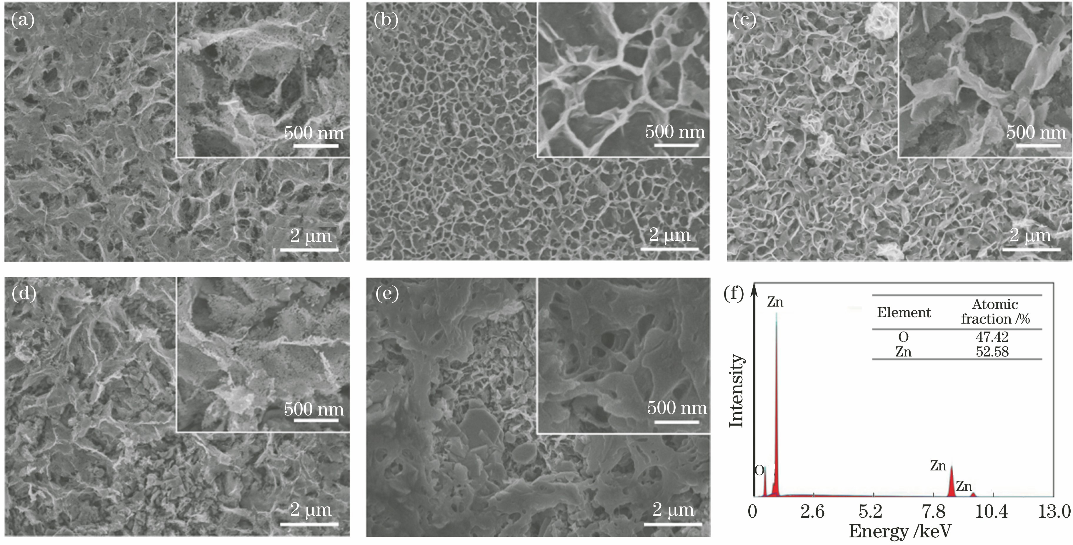
    Fig. 2. SEM images of ZnO nanowalls grown at different deposition voltages and EDS spectrum of ZnO nanowalls grown at deposition voltage of 1.6 V. (a) 1.4 V; (b) 1.6 V; (c) 1.8 V; (d) 2.0 V; (e) 2.2 V; (f) EDS spectrum
    XRD patterns of ZnO nanowalls grown at different deposition voltages
    Fig. 3. XRD patterns of ZnO nanowalls grown at different deposition voltages
    Raman spectra of ZnO nanowalls grown at different deposition voltages
    Fig. 4. Raman spectra of ZnO nanowalls grown at different deposition voltages
    Photoluminescence spectra of ZnO nanowalls grown at different deposition voltages
    Fig. 5. Photoluminescence spectra of ZnO nanowalls grown at different deposition voltages
    Transmittance spectra of ZnO nanowalls and seed crystal substrate
    Fig. 6. Transmittance spectra of ZnO nanowalls and seed crystal substrate
    Ultraviolet response characteristic diagrams of ZnO nanowalls. (a) UV response curves of ZnO nanowalls; (b) response and recovery curve of ZnO nanowalls at deposition voltage of 1.6 V; (c) UV response and recovery time of ZnO nanowalls versus deposition voltage
    Fig. 7. Ultraviolet response characteristic diagrams of ZnO nanowalls. (a) UV response curves of ZnO nanowalls; (b) response and recovery curve of ZnO nanowalls at deposition voltage of 1.6 V; (c) UV response and recovery time of ZnO nanowalls versus deposition voltage
    I-V characteristics of ZnO nanowalls. (a) I-V characteristics of ZnO nanowalls at deposition voltage of 1.6 V; (b) photo-to-dark current ratio of ZnO nanowalls versus deposition voltage
    Fig. 8. I-V characteristics of ZnO nanowalls. (a) I-V characteristics of ZnO nanowalls at deposition voltage of 1.6 V; (b) photo-to-dark current ratio of ZnO nanowalls versus deposition voltage
    Shiguang Shang, Lang Gao, Wei Ren, Wenqian Zhang, Rui Wang. Fabrication of ZnO Nanowalls by Electrochemical Deposition and Ultraviolet Detection Performance[J]. Acta Optica Sinica, 2021, 41(7): 0716001
    Download Citation