
Yue Wang, Yanbing Leng, Lianhe Dong, Li Wang, Shunrui Liu, Jun Wang, Yanjun Sun. Design of Tunable Metamaterial Absorber Based on Graphene-Metal Hybrid Structure[J]. Acta Optica Sinica, 2018, 38(7): 0716001
- Acta Optica Sinica
- Vol. 38, Issue 7, 0716001 (2018)
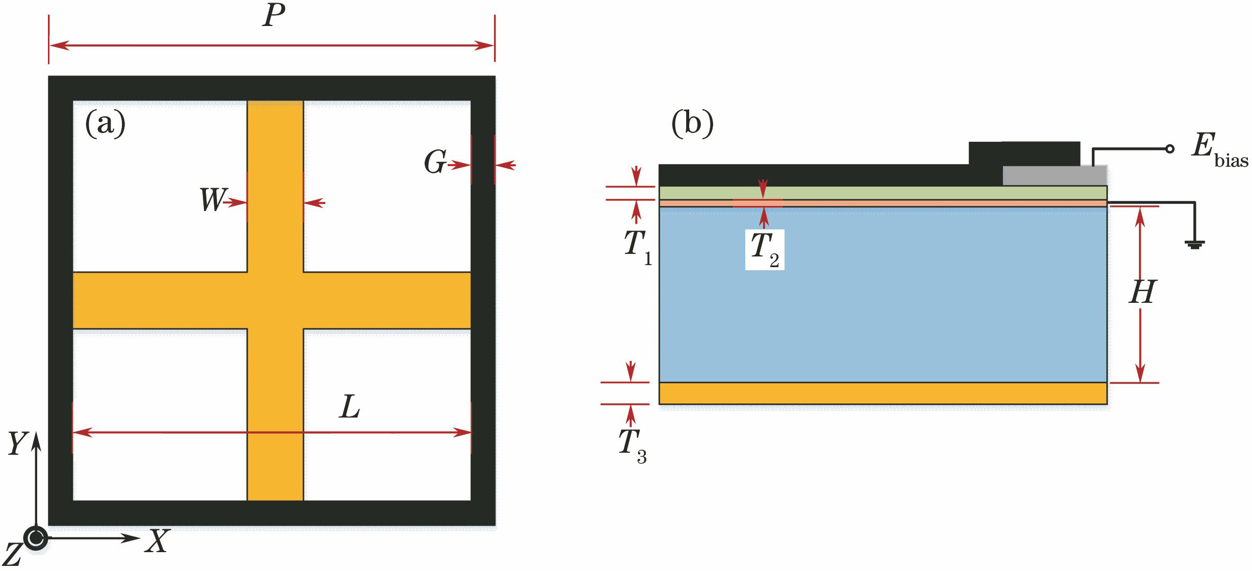
Fig. 1. Structural diagram of metamaterial absorber based on graphene-metal hybrid. (a) Top view of unit structure; (b) front view of structure
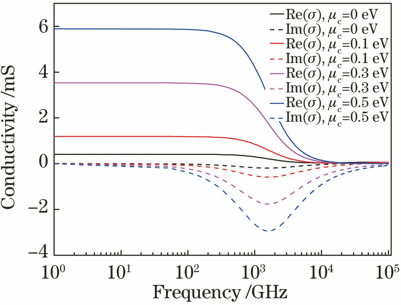
Fig. 2. Conductivity cures of graphene with different Fermi levels
Fig. 3. Absorptivity curves of different structures. (a) Single metal cross structure, single graphene structure, and graphene-metal hybrid structure; (b) metamaterial absorbers with different Fermi levels
Fig. 4. Absorptivity curves under different graphene widths
Fig. 5. Schematic of unit structure of broadband metamaterial absorber based on graphene-metal hybrid structure
Fig. 6. Absorptivity curves of broadband metamaterial absorbers with different Fermi levels
Fig. 7. Field distributions of metamaterial absorber when graphene Fermi level is 0 eV. (a) Surface current, graphene-metal hybrid structure; (b) surface current, metal substrate; (c) electric field, graphene-metal hybrid structure
Fig. 8. Field distributions of metamaterial absorbers with different structures when graphene Fermi level is 0 eV. (a) Single metal cross structure; (b) single graphene structure; (c) graphene-metal hybrid structure
Fig. 9. Field distributions of metamaterial absorber when graphene Femi level is 0.3 eV. (a) Surface current, graphene-metal hybrid structure; (b) surface current, metal substrate; (c) electric field, graphene-metal hybrid structure
Fig. 10. Field distributions of metamaterial absorber under different frequencies when graphene Fermi level is 0 eV. (a) 28 GHz; (b) 32 GHz

Set citation alerts for the article
Please enter your email address
© Copyright 2018-2021 | Chinese Laser Press. All Rights Reserved 沪ICP备15018463号-20