
Jinhyeong Yoon, Jae-Yong Kim, Junhyeong Kim, Hyeonho Yoon, Berkay Neşeli, Hyo-Hoon Park, Hamza Kurt. Inverse design of a Si-based high-performance vertical-emitting meta-grating coupler on a 220 nm silicon-on-insulator platform[J]. Photonics Research, 2023, 11(6): 897
- Photonics Research
- Vol. 11, Issue 6, 897 (2023)
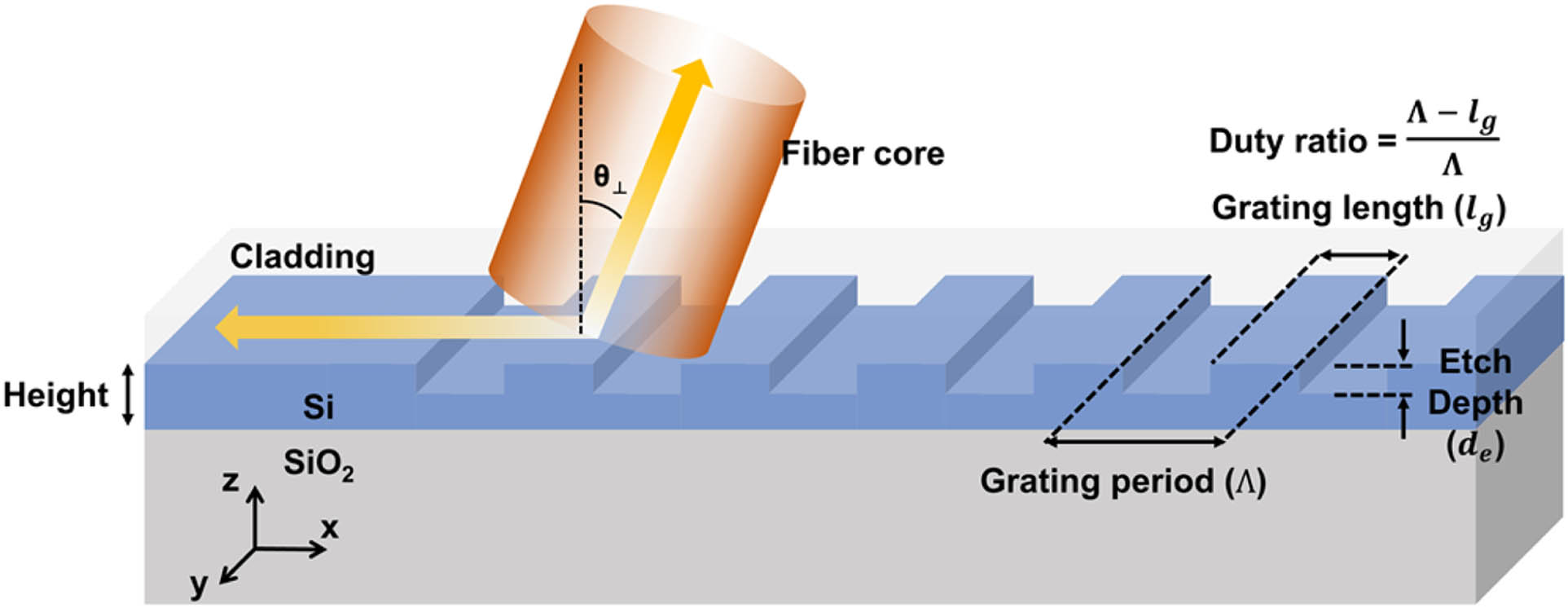
Fig. 1. Fundamental schematic of the uniform Si grating coupler. θ ⊥
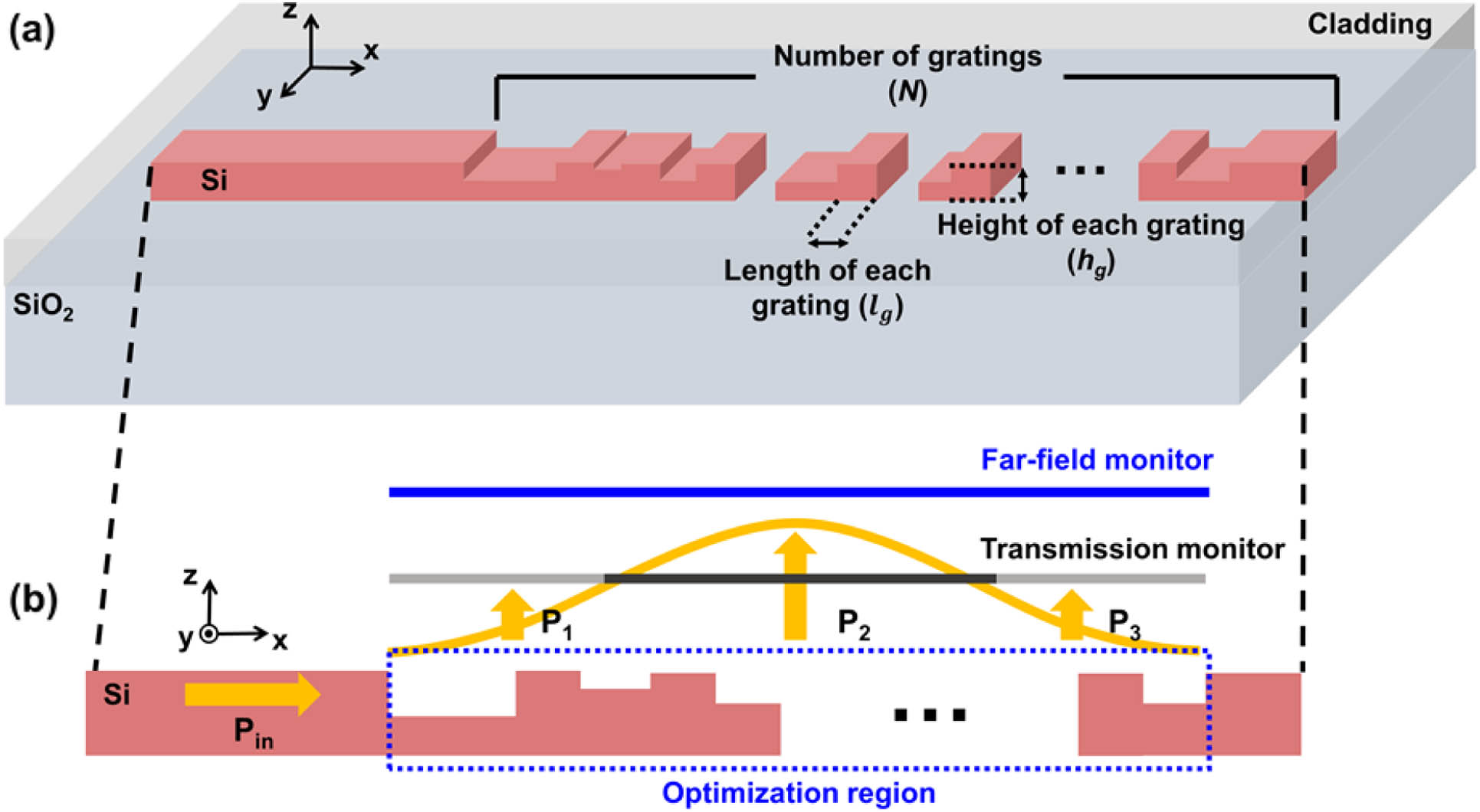
Fig. 2. (a) Optimization parameters used in the analysis. (b) The objective power distribution of emitted light for high outcoupling efficiency.
Fig. 3. (a) Result of the optimized meta-grating structure with a disconnected region surrounded by connected regions. The L-shape and U-shape grating elements in the middle section (disconnected region) appear as a consequence of the inverse design optimization. (b) Field distribution profile of the optimized meta-grating coupler (purple line) and that of Gaussian beam (green dotted line) guided in single-mode fiber. The far-field pattern of the designed meta-grating coupler in (c) 2D FDTD simulation and (d) 3D FDTD simulation at the center wavelength (1556 nm).
Fig. 4. (a) Power fraction of upward (blue line), downward (red line), and reflection (black line) directions calculated using the FDTD simulation. (b) Simulated fiber-to-chip vertical coupling loss of FDTD analysis.
Fig. 5. (a) Height distribution of inverse design-optimized grating coupler. (b) Cross-section view of the modified meta-grating coupler for fabrication.
Fig. 6. (a) Simulated fiber-to-chip vertical coupling loss results with the modified meta-grating coupler. (b) Far-field distribution of the modified meta-grating coupler in the FDTD simulation at the center wavelength (1566 nm).
Fig. 7. (a) Microscopy image, (b) scanning electron microscopy image, and (c) cross-section of a fabricated meta-grating coupler.
Fig. 8. Experimentally measured chip-to-fiber coupling loss of a fabricated silicon meta-grating coupler.
Fig. 9. (a) Wave-vector diagram for the suggested grating coupler. β K z -direction, and k 0
|
Table 1. Comparison between the Different Perfectly Vertical Grating Couplers with the 220 nm Si Thickness

Set citation alerts for the article
Please enter your email address
© Copyright 2018-2021 | Chinese Laser Press. All Rights Reserved 沪ICP备15018463号-20