Jinhyeong Yoon, Jae-Yong Kim, Junhyeong Kim, Hyeonho Yoon, Berkay Neşeli, Hyo-Hoon Park, Hamza Kurt, "Inverse design of a Si-based high-performance vertical-emitting meta-grating coupler on a 220 nm silicon-on-insulator platform," Photonics Res. 11, 897 (2023)
Copy Citation Text
Efficient extraction of light from a high refractive index silicon waveguide out of a chip is difficult to achieve. An inverse design approach was employed using the particle swarm optimization method to attain a vertical emitting meta-grating coupler with high coupling efficiency in a 220-nm-thick silicon-on-insulator platform. By carefully selecting the figure of merit and appropriately defining parameter space, unique L-shape and U-shape grating elements that boosted the out-of-plane radiation of light were obtained. In addition, a 65.7% () outcoupling efficiency and a 60.2% () fiber-to-chip vertical coupling efficiency with an 88 nm 3 dB bandwidth were demonstrated by numerical simulation. Considering fabrication constraints, the optimized complex meta-grating coupler was modified to correspond to two etching steps and was then fabricated with a complementary metal-oxide-semiconductor-compatible process. The modified meta-grating coupler exhibited a simulated coupling efficiency of 57.5% () with a 74 nm 3-dB bandwidth in the C-band and an experimentally measured coupling efficiency of 38% ().
1. INTRODUCTION
Silicon photonics has emerged as a promising technology in various fields, including optical communication, light detection and ranging, quantum computing, and sensing. With an increased demand for low-cost and highly integrated optical devices, the silicon photonics platform has become a major candidate, able to satisfy the requirements of a complementary metal-oxide-semiconductor (CMOS)-compatible process and high integration with chip-scale footprint.
The coupling technology between a Si chip and an optical fiber is the most fundamental silicon photonics technology of the silicon-on-insulator (SOI) platform. There are several technologies for coupling light in a Si chip, including edge coupler, end-fire coupler, and grating coupler [1–3]. However, the edge coupler has some restrictions in that it must be located at the chip facets, which makes it hard to test devices at the wafer scale. Although the end-fire coupler avoids this limitation, advanced manufacturing technology is required. Consequently, the grating coupler is commonly employed in silicon photonics platforms because of its straightforward manufacturing process and potential for improvement.
A number of previous studies have been conducted to improve the coupling efficiency and directivity of the grating coupler. The grating coupler coupling efficiency is related directly to its directivity, which is also known as directionality. One straightforward method to improve the upward directivity of a grating coupler is to use bottom reflection via dielectric multilayers or a metallic mirror [4–9]. Additionally, it has been demonstrated that utilizing a non-uniform grating structure [10–18] for apodization can improve the coupling efficiency. Other approaches have employed modified grating structures, such as multiple etch-depth levels [19–25], slanted or blazed grating structures [26–29], and overlay for high-contrast gratings [30–32]. Recently, the inverse design approach has been widely used for grating couplers designing [33–38].
Sign up for Photonics Research TOC. Get the latest issue of Photonics Research delivered right to you!Sign up now
Packaging between chips and surface-emitting lasers such as vertical-cavity surface-emitting lasers can be made more effective by using a vertical grating coupler. When employing the grating coupler as an optical antenna, vertical coupling or emitting is another solution that can improve the longitudinal steering angle of an antenna. However, because of reflection, the directivity of the vertically emitted grating coupler is restricted. To fulfill both vertical coupling and high directivity, several other solutions have been investigated [39–44].
The directionality of the grating coupler depends on the thickness of the Si waveguide, and it tends to increase as the thickness of the Si waveguide layer increases. Previous research has improved the directionality of the grating couplers, usually using Si waveguide layers with various thicknesses . For example, in Refs. [6,7], the backside metallic mirror was used to increase the upward directivity of the grating coupler in a 250 nm silicon-layer platform. In Ref. [15], the authors investigated numerically and experimentally a 260-nm-thick SOI platform to produce a highly efficient grating coupler. The neural network-based inverse design method was employed in a 280-nm-thick silicon grating coupler design in Ref. [35]. Finally, in Ref. [38], a vertical grating coupler with a 340 nm top silicon height design using a binary search algorithm was demonstrated.
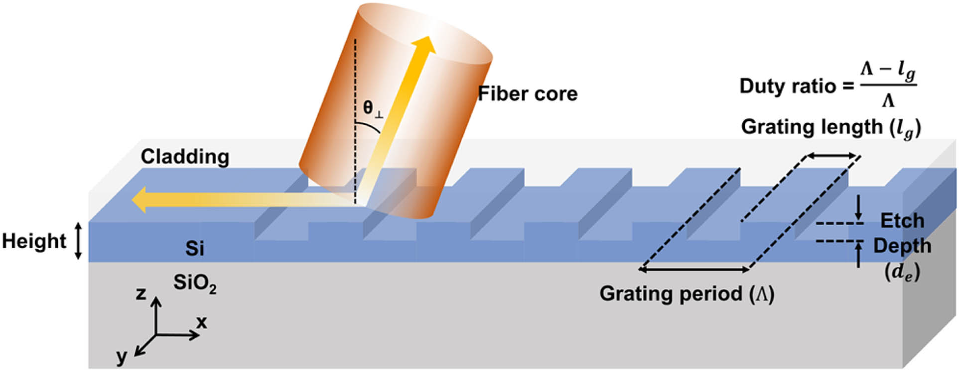
Nonetheless, a 220-nm-thick SOI with an appropriate waveguide width such as 500 nm is commonly used in silicon photonics as a standard. It allows only a single mode of light and has low loss in O-band and C-band. It is notably challenging in silicon photonics to improve the vertical coupling efficiency of a grating coupler with a 220 nm thickness. A usual approach is based on a forward design by mainly focusing on the parameters of the grating coupler, and changing the grating period to a non-uniformly varying one, or using multi-etch depth parameters, as schematically shown in Fig. 1.
Figure 1.Fundamental schematic of the uniform Si grating coupler. indicates the diffraction angle of the grating coupler equal to the coupling angle between the optical fiber and surface normal to the grating. The coupling angle is determined by the refractive index of the Si waveguide, grating period, and operating wavelength. The coupling can be bi-directional between the grating coupler and a fiber. The schematic is not drawn to scale.
In this paper, we propose and investigate an atypical meta-grating coupler that has both vertical emission property and high coupling efficiency, and it was designed using the inverse design method. We targeted a grating coupler that provides strong directivity by means of the height variation of each scattering element, causing the direction of the guiding mode to be vertically emitted. Here we suggest a meta-grating coupler designed with the particle swarm optimization (PSO) algorithm in a 220-nm-thick SOI platform, having two etching levels considered CMOS fabrication processes. In a recent study [42], a high-efficiency grating coupler including a polysilicon overlay was designed using high-index contrast characteristics utilizing polysilicon overlay that requires an additional polysilicon deposition fabrication process. It is important to note that the present grating coupler is to be fabricated using the CMOS fabrication process due to its low cost and general fabrication process. According to Refs. [43,44], the authors have designed an efficient grating coupler using a novel design and multi-etch process. Our designed grating coupler differs from this design in that we have fabricated and experimentally verified the designed grating coupler. In addition, even though a similar optimization method was used in both designs, our designed grating coupler was based on a random structure rather than a periodic or regular one. A number of grating couplers have been designed with periodic structures, and they have been verified in many studies. However, there have been only a few studies of random structure-based grating couplers. Thus, the originality in our design is because we demonstrate the high performance of a random structure-based inverse-designed grating coupler. We also succeeded in increasing the coupling efficiency of the grating coupler through a design that differed from previous studies by using a unique set of figures of merit. A well-defined figure of merit in terms of generating a Gaussian profile and vertical emitting can be a powerful and original characteristic of our design. Finally, the outcome of the optimization method searching parameter space provided a set of grating elements that can be grouped into either L-shape or U-shape types because the majority of the grating heights are restricted to three values.
2. DESIGN AND SIMULATION OF THE META-GRATING COUPLER
The formulation of the design tools and crucial parameters are important. In our inverse design, we used the particle swarm optimization algorithm, supported by the finite difference time domain (FDTD) simulation tool [45]. The PSO method is a widely used algorithm in device designs. By creating multiple particles and updating their positions and velocity during iterations, the PSO identifies the optimal particles. The optimization is performed according to the defined figure of merit, which is an objective function determined by the user. Figure 2(a) shows the design variables, namely the height of the grating, the length of the grating, and the total number of gratings. The height of each grating () is not fixed, as shown in Fig. 2(a). It is important to take the possible use of cost-effective CMOS fabrication into account when designing a complex grating coupler. Because of the resolution of the photolithography process, we fixed the length of each meta-grating () to 200 nm. It should be noted that 100 nm or even smaller values are possible with extreme-UV photolithography or electron-beam lithography. As the design must also consider the diameter of the optical fiber core, the number of meta-gratings/scatterers (N) was set to 90, which corresponds to a total length of 18 μm. For a 220-nm-thick SOI platform, each meta-grating had a height variance between 0 and 220 nm. A meta-grating coupler composed of 90 random heights of gratings is used as one particle in the PSO algorithm in our design.
Figure 2.(a) Optimization parameters used in the analysis. (b) The objective power distribution of emitted light for high outcoupling efficiency.
The optimization process focused on enhancing the coupling efficiency of the meta-grating coupler with a vertical emission. Since the coupling efficiency is affected by the directivity of the grating coupler and the field profile of the emitted beam, the figure of merit (FOM) of the optimization should include the divided directivity terms as shown in the following equation:
Equation (1) shows the first considering only the directivity and field distribution of the out-of-plane waveguide mode. Because we divided the transmission monitor into three sections, the field distribution of the upward beam should be determined by three terms, as shown in Eq. (1). is the total input power of the waveguide mode; , , and are the emitted power from each part of the radiating section, as shown in Fig. 2(b). The coefficients , , and are selected to allow efficient field distribution of the upward emitted beam. As a result of numerous optimization attempts, we were able to obtain an optimal coefficient value for a Gaussian profile. If the number of divided sections increases, the obtained profile may be further improved. However, the optimization process can be complicated, and more time may be required to optimize when the number of transmission monitors increases. Hence, we set the number of monitors as three considering this trade-off. Here, while the reciprocity theorem can be applied to any type of grating couplers, we only consider the coupling efficiency of the output configuration in our work [1,46]. The following equation of as a second FOM includes the far-field profile to optimize the structure for vertical emission:
In Eq. (2), and indicate the intensity of the far-field profile at the (, ) position and the selected coefficient, respectively. The far-field profile can be obtained with a far-field projection monitor, as shown in Fig. 2(b). The emission angle can be obtained using the (, ) coordinate of far-field profile results in FDTD simulation. Furthermore, to obtain the perfect vertical emission profiles, we set the (, ) coordinate as (0,0). Thus, the total FOM was decided by the addition of and .
Figure 3 shows the optimization results of the designed meta-grating coupler and the simulated directivity and field distribution result of the optimized structure. The optimized meta-grating coupler consists of a disconnected region surrounded by connected regions, as shown in Fig. 3(a). The strong radiation of the guided light occurs over the disconnected region and less power is coupled within the connected regions. This indicates the success of the inverse design method, providing unique meta-grating elements for a total of 90 gratings. The heights of the gratings in the connected region vary from 150 nm to 220 nm, and those in the disconnected region vary from 0 nm to 220 nm. Because we set the coefficients in Eq. (1) to have a Gaussian distribution, which is similar to the field profile of a single-mode fiber, a small amount of scattering occurs in the connected regions while the large scattering occurs in the disconnected region. Hence, a Gaussian-like field distribution can be obtained as shown in Fig. 3(b), and it can improve the coupling efficiency between the designed meta-grating coupler and single-mode fiber.
Figure 3.(a) Result of the optimized meta-grating structure with a disconnected region surrounded by connected regions. The L-shape and U-shape grating elements in the middle section (disconnected region) appear as a consequence of the inverse design optimization. (b) Field distribution profile of the optimized meta-grating coupler (purple line) and that of Gaussian beam (green dotted line) guided in single-mode fiber. The far-field pattern of the designed meta-grating coupler in (c) 2D FDTD simulation and (d) 3D FDTD simulation at the center wavelength (1556 nm).
In addition, we can obtain vertical emission at the center wavelength with a designed meta-grating coupler, as shown in Figs. 3(c) and 3(d) with a small back-reflected light in the waveguide. The anti-reflection condition occurs at the center wavelength of 1556 nm, and high vertical radiation can be achieved at the same wavelength. In Fig. 3(c), the aperiodicity of the grating heights causes an increase in sidelobes and asymmetry in the far-field profile. However, the vertical emission with a peak intensity at zero angle was obtained, as we targeted in Eq. (2).
Figure 4(a) shows the power fraction of each propagation direction, upward, downward, and reflection backward. The upward directivity was 65.7% () at 1556 nm wavelength, while downward and reflection directivities were about 34.1% and 0.2%, respectively. In addition, most of the light passing through the meta-grating coupler is emitted upward or downward, so only a small amount of light remains within the meta-grating coupler. This high outcoupling efficiency can also help improve fiber-to-chip coupling efficiency, and we expect the further improvement of upward directivity using bottom reflection for the downward propagating light, by means of either dielectric multilayers or metallic mirrors.
Figure 4.(a) Power fraction of upward (blue line), downward (red line), and reflection (black line) directions calculated using the FDTD simulation. (b) Simulated fiber-to-chip vertical coupling loss of FDTD analysis.
The calculated fiber-to-chip vertical coupling efficiency (or vertical coupling loss) of the proposed meta-grating coupler is shown in Fig. 4(b). In the FDTD simulation, the result of coupling efficiency was 60.2% () at the 1556 nm wavelength, and 3-dB bandwidth () at 88 nm, which indicates lower coupling loss than the conventional grating coupler in vertical coupling condition. This implies that the Gaussian-like propagating mode is effectively confined in single-mode fiber thanks to a well-defined and implemented FOM.
3. FABRICATION AND EXPERIMENTAL MEASUREMENT
Although the suggested complex meta-grating coupler has several benefits in terms of coupling efficiency and bandwidth, its fabricating may be challenging. Figure 5(a) shows the height variation of the optimized grating coupler. As we can see from the plot, most of the gratings have 0 nm (full-etch), 150 nm, and 220 nm (no-etch) heights. This is another success of the algorithm in that the grating heights are not uniformly or totally randomly distributed, but the three height values dominate. While the majority of the heights were restricted to these three values, the heights of all gratings were adjusted among one of these three levels, as shown in Fig. 5(b). This modified structure can be fabricated with CMOS fabrication without any additional etching process.
Figure 5.(a) Height distribution of inverse design-optimized grating coupler. (b) Cross-section view of the modified meta-grating coupler for fabrication.
Because changes in height lead to changes in the refractive index of each grating, this means the center wavelength of the modified meta-grating coupler will be changed. Figure 6 shows the simulated coupling efficiency and far-field pattern result of the modified meta-grating coupler. The simulated fiber-to-chip vertical coupling efficiency of the modified meta-grating coupler is about 57.5% () at 1566 nm of wavelength. The main wavelength is shifted, and the coupling efficiency is slightly lower compared with the early optimized structure. The 3-dB bandwidth decreased from 88 nm to 74 nm, which implies that a large dispersion occurs in the modified structure. With this modified meta-grating coupler, we still can obtain both vertical emission and high coupling efficiency at the main operating wavelength, as shown in Figs. 6(a) and 6(b).
Figure 6.(a) Simulated fiber-to-chip vertical coupling loss results with the modified meta-grating coupler. (b) Far-field distribution of the modified meta-grating coupler in the FDTD simulation at the center wavelength (1566 nm).
The grating coupler employing the modified meta-grating structure was fabricated using a CMOS-compatible fabrication process. An 8-inch SOI wafer with a top silicon thickness of 220 nm was used in the fabrication. As only two etching steps are needed to fabricate this grating coupler, a KrF scanner with a 248 nm wavelength laser was used for the photolithography, with two etching steps. An oxide hard mask covered the part of the top silicon layer, which has 220-nm-heigh gratings, and 70 nm and 220 nm etchings were conducted for the 150 nm and 0 nm height gratings. 10 μm was adopted as the y-direction width of the grating coupler, which corresponds to the width of the mode field diameter of single-mode fiber. Thus, the total footprint of the fabricated grating coupler is μμ, and the microscopy images are shown in Fig. 7. The mode conversion between the single-mode waveguide and grating coupler was accomplished by the 500 μm length of the tapered waveguide. It should be noted that mode converting can be accomplished by adopting a focusing grating coupler [47]. Additionally, the measured waveguide loss is 1.8 dB/cm.
Figure 7.(a) Microscopy image, (b) scanning electron microscopy image, and (c) cross-section of a fabricated meta-grating coupler.
Figure 8 shows the experimental result of the fabricated grating coupler. The peak coupling efficiency at the center wavelength was 38% () and the 3-dB bandwidth was 48 nm, which is less than the numerically calculated data. Note that the length of each grating was 200 nm, and the critical dimension of the fabrication process was almost 200 nm. Fabrication errors can occur in the etching process and may cause a difference between the simulation result and the measured data. Even with two etching processes, a mask misalignment may occur during the photolithography process. Hence, some meta-gratings had different grating length and height from what we intended, as clearly shown in Fig. 7(c). The reproducibility of such multi-level complex meta-gratings is highly challenging and depends on fabrication technology. Based on the results of measurement performed on more than ten samples, we obtained approximately a 10% repeatability in the fabrication process. In addition, the increased randomness of the structure due to fabrication error generated obvious oscillation appearing over the coupling efficiency curve.
Figure 8.Experimentally measured chip-to-fiber coupling loss of a fabricated silicon meta-grating coupler.
The two main fabrication errors causing degradation in coupling efficiency are the incorrect mask alignment of two etching masks and the over-etching depth of each meta-grating. The used equipment for the photolithography process has 180 nm of critical dimension and 50 nm of alignment accuracy. Thus, the fabrication tolerance of the designed structure is moderate due to this photolithography equipment. As can be seen from Fig. 7(c), undesired etching occurs in some parts due to mask misalignment. In addition, it can be seen that over-etching occurs at the front part of the structure, resulting in a grating with a height of about 50 nm rather than a grating with a height of 150 nm. The typical sidewall angle is calculated as 71° within a range of 38° to 80° variations, which may also cause a decrease in the performance of the fabricated meta-grating coupler. These fabrication errors can reduce the coupling efficiency of the grating coupler, while generating a shift in center wavelength [30].
However, these fabrication errors can be improved by using a more sophisticated fabrication process. For instance, the high etching resolution employed by electron-beam (E-beam) lithography can help the elaborate fabrication of the designed meta-grating coupler. In addition, it is possible to achieve a better fabrication tolerance and mass production of the designed structure using elaborate lithography methods such as extreme ultraviolet lithography or nanoimprint lithography. It is also possible to apply an inverse design approach to design a fabrication error-tolerant grating coupler by accounting for mask misalignment and over-etching issues [48].
4. DISCUSSION
The optimized meta-grating coupler can be analyzed using a wave-vector diagram, as shown in Fig. 9. In Fig. 9(a), and indicate the refractive indices of the low-index material and the high-index material, respectively. For a periodic grating structure, the grating vector along the z-direction (K) is determined by the grating period () of the structure, while the propagation constant of waveguide mode () is determined by the center wavelength () and effective index () of the structure. Vertical emission of the meta-grating coupler occurs when the propagation constant and grating vector have the same value. Therefore, we first calculated the effective index of the optimized grating coupler using the MODE simulation tool [45]. Since the designed grating coupler has various grating heights, with dimensions , where h is the height, the effective index of each grating was calculated, as shown in Fig. 9(b). Then, the average effective index can be obtained by averaging the value of the effective index distribution according to the height of each meta-grating.
Figure 9.(a) Wave-vector diagram for the suggested grating coupler. is the propagation constant of the waveguide mode, is the grating vector along the z-direction, and is the wave vector of out-of-plane light. (b) Simulation result of refractive index difference with respect to height variation of the grating element.
The calculated average effective index of the proposed grating coupler was determined to be about 2.48. In addition, the vertical coupling occurs at 1556 nm for the center wavelength. Hence the average grating period () can be estimated at 627 nm by the diffraction grating formula described by Eq. (3). In Eq. (3), indicates the emission angle of a grating coupler while and indicate the operating wavelength and period of a grating coupler, respectively:
As the length of each meta-grating is 200 nm, more than three gratings work as one period of the optimized grating coupler. This implies that we can achieve vertical coupling with a non-periodic series of gratings 200 nm in length, rather than periodic gratings of 627 nm. Furthermore, this non-periodicity can suppress the back reflection of the light, while achieving vertical coupling.
The benefit of the inverse design approach is that it allows the exploration of a large amount of parameter space to target challenging objectives that are quite difficult to achieve with a trial-and-error method. One can alter the FOMs to obtain other functionalities in the on-chip platform and change the material type as well. Such cases can also be implemented with the present inverse design technique.
5. CONCLUSION
In conclusion, we demonstrated a vertical meta-grating coupler with high coupling efficiency designed using the inverse design method for a standard 220 nm SOI platform. The optimized meta-grating coupler yields 65.7% of simulated outcoupling efficiency at a center wavelength of 1556 nm, and fiber-to-chip vertical coupling efficiency of 60.2% () with a 3-dB bandwidth of 88 nm. To fabricate the optimized grating coupler using a CMOS compatible process, the meta-grating coupler was modified to have three height levels. The simulated coupling efficiency of the modified meta-grating coupler was 57.5% () at a shifted center wavelength of 1566 nm, with a 3-dB bandwidth of 74 nm. The measured coupling efficiency of the fabricated grating coupler was 38% (). These differences in numerical and measured data are caused by fabrication errors, which can be improved by applying a more sophisticated nanofabrication method and considering smaller feature sizes. Despite the fabrication errors, the designed meta-grating coupler is effective in vertical coupling compared to other research, while considering the 220 nm Si thickness (see Table 1). The proposed meta-grating coupler has a wide bandwidth and a reasonable coupling efficiency with a relatively large feature size of 200 nm, requiring only two fabrication steps. We believe that we can achieve even a highly efficient and broad-band meta-grating coupler through the additional structure optimization with a smaller feature size and defining a different figure of merit. Furthermore, through several fabrication trials, a meta-grating coupler with high fabrication tolerance can be designed by carefully determining the linewidth compensation parameter that can compensate for fabrication errors. This novel meta-grating structure has a potential for further improvement with other inverse design methods [49,50], which is useful for various applications in silicon photonics.
Comparison between the Different Perfectly Vertical Grating Couplers with the 220 nm Si Thickness
Structure Description
Simulated/Experimental Coupling Efficiency (%)
3-dB Bandwidth (nm)
Feature Size (nm)
Footprint (μ)
Fabrication Step
References
Chirped
42/34
48
307
2
[39]
Tilteda
39.3/28.5
62
275
[40]
Dual-etch
45.3/27.6
68
188
2
[41]
Poly-Si overlaya
81.1/71.6
48
180
[42]
Meta-material
72/–
78
106
2
[43]
Meta-grating coupler
60.2/38
88
200
2
This work
The presented footprint of the grating coupler includes focusing or linear taper region.
[5] S. K. Selvaraja, D. Vermeulen, M. Schaekers, E. Sleeckx, W. Bogaerts, G. Roelkens, P. Dumon, D. Van Thourhout, R. Baets. Highly efficient grating coupler between optical fiber and silicon photonic circuit. Conference on Lasers and Electo-Optics/International Quantumm Electronics Conference, CTuC6(2009).
[17] C. Chang, Y. Hsu, H. Kuo, Y. Lai. Subwavelength apodized grating coupler for silicon photonics waveguide coupling. Opto-Electronics and Communications Conference, 1-3(2020).
[19] M. Fan, M. A. Popović, F. X. Kärtner. High directivity, vertical fiber-to-chip coupler with anisotropically radiating grating teeth. Conference on Lasers and Electro-Optics (CLEO), CTuDD3(2007).
[24] L. Cheng, X. Mu, S. Wu, X. Tu, H. Y. Fu. Perfectly vertical grating coupler for O and C-band. Frontiers in Optics + Laser Science APS/DLS, JW4A.57.S(2019).
Jinhyeong Yoon, Jae-Yong Kim, Junhyeong Kim, Hyeonho Yoon, Berkay Neşeli, Hyo-Hoon Park, Hamza Kurt, "Inverse design of a Si-based high-performance vertical-emitting meta-grating coupler on a 220 nm silicon-on-insulator platform," Photonics Res. 11, 897 (2023)