
Li Liu, Ruxue Wang, Xuyi Zhao, Wenfu Yu, Yi Jin, Qian Gong, Aimin Wu, "Heterogeneously integrated quantum-dot emitters efficiently driven by a quasi-BIC-supporting dielectric nanoresonator," Photonics Res. 10, 1971 (2022)
- Photonics Research
- Vol. 10, Issue 8, 1971 (2022)
Abstract
1. INTRODUCTION
Silicon photonics has been widely used in optical interconnection for telecom and datacom, as well as biosensing, while on-chip light sources are still a major challenge for high-density and low-cost integration. In contrast with silicon, III-V materials provide ideal gain properties. Hybrid lasers using III-V materials through the flip-chip technology [1] and the heterogeneous bonding technology [2] have been proven successful. The heterogeneous bonding technology provides robust alignment and post-CMOS process flexibility, as another promising scheme, and high-performance III-V quantum dots (QDs) [3,4] directly grown on silicon substrates by molecular beam epitaxy (MBE) technology [5] can enable cost-effective integration of low-threshold optical sources on silicon.
The development of nanophotonics makes it ready for developing ultracompact on-chip sources on the other side. By confining light to a small volume based on localized resonance, subwavelength nanoresonators hold great promise [6,7]. Compared to metal nanoresonators, dielectric ones are preferred, since the material loss is negligible. Some innovative methods have been raised to design resonant dielectric nanoresonators [8] based on multipolar resonance [9–13]. Multipolar resonance makes a dielectric nanoresonator possess rich resonating ways, but it is weak in confining optical energy so that the corresponding quality factor (
In this work, we propose to introduce the advantages of III-V QDs into a quasi-BIC-supporting dielectric nanodisk to construct a small on-chip bright light source. However, there are some parasitic problems if one directly grows III-V QDs on a silicon substrate. The different properties of thermal expansion and polarity existing between III-V and silicon materials may result in a high density of crystalline defects [31,32]. A relatively thick III-V buffer layer grown on a V-groove-patterned (001) silicon substrate [33–36] is often used to overcome this mismatch, but this may cause the formation of thermal crack that may degrade the above III-V epilayer and induce the reliability issue in practical application. In addition, such a thick buffer layer may weaken the coupling from the active region to a silicon waveguide [37]. Here, we will combine the III-V-QD epitaxy and heterogenous bonding technologies. Based on such a combination, an individual quasi-BIC-supporting GaAs nanoresonator with embedded InAs QDs will be constructed. This architecture can improve the coupling between the QDs and the supported quasi-BIC to enhance the photoluminescence (PL).
Sign up for Photonics Research TOC. Get the latest issue of Photonics Research delivered right to you!Sign up now
2. RESULTS AND DISCUSSION
A single subwavelength dielectric nanodisk, supporting a quasi-BIC via the strong coupling between a Mie-like resonant mode and a Fabry–Perot (FP)-like resonant mode, can be designed following the Friedrich–Wintgen interference mechanism [21].
To briefly illustrate the physical mechanism of the quasi-BIC formation, scattering simulation and
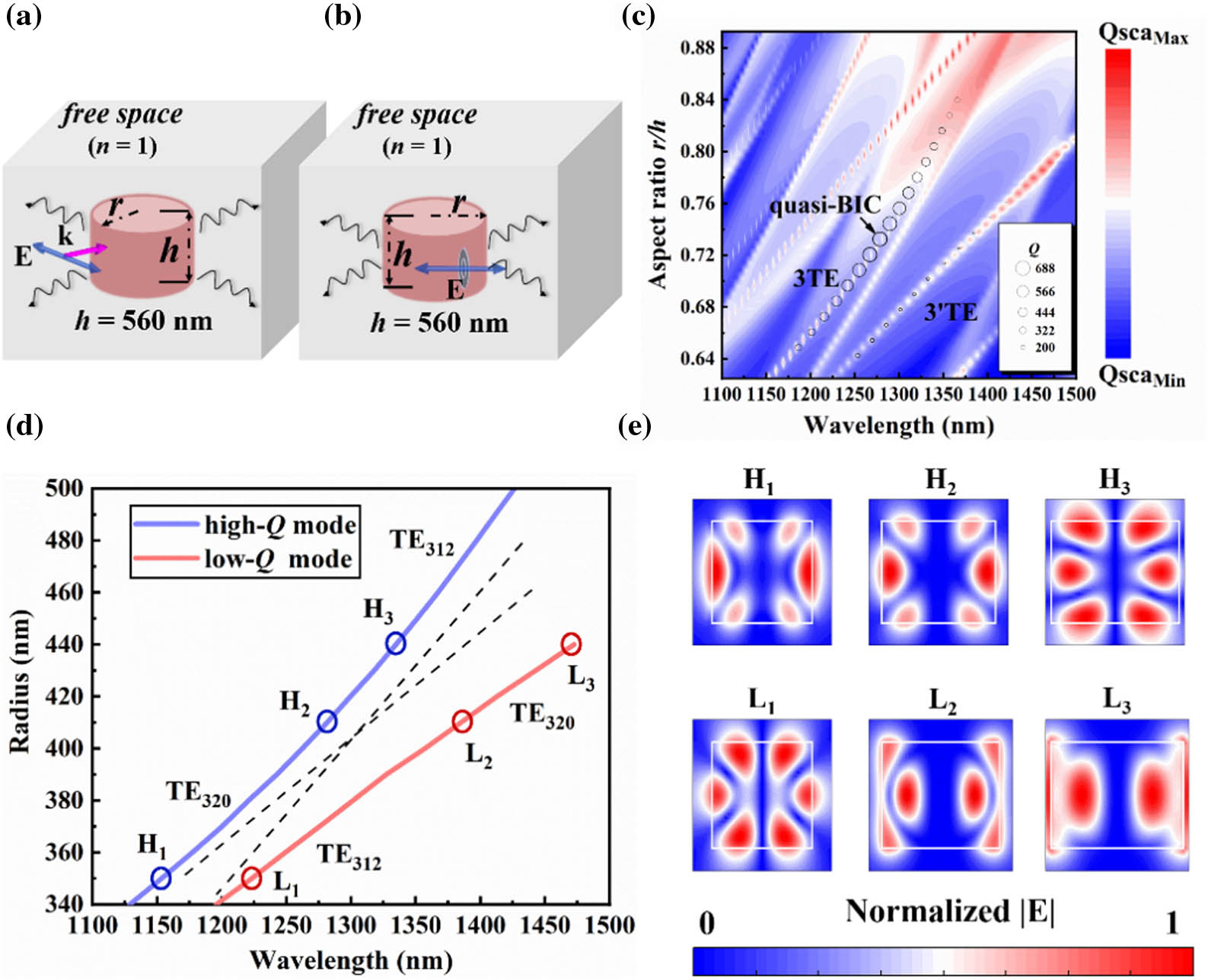
Figure 1.Resonating and scattering behavior of a single GaAs nanodisk. (a), (b) Schematic of the dielectric nanodisk in free space for scattering (a) and
When a transverse electric (TE) plane wave impinges on the nanodisk (the incident magnetic field is polarized along the cylinder axis), the scattering cross section as a function of the aspect ratio of the nanodisk (defined as
For clearer illumination, the resonant modes corresponding to the two labeled bright stripes are extracted and represented by two solid anticrossing curves corresponding to high-
A high-
![]()
Figure 2.Fabricating GaAs nanodisks with embedded InAs QDs. (a) Growing InAs QDs. An active multilayer is grown on a GaAs (100) substrate by MBE, between which there is a 500 nm GaAs buffer layer and a 500 nm AlAs sacrificial layer. The active multilayer consists of a 275 nm GaAs bottom cladding layer, 10 nm InAs dot-in-well gain material (2 nm
According to the atomic force microscope (AFM) measurement shown in Fig. 2(g), one can see that the surface roughness of the transferred active multilayer is no more than 10 nm, and the change of the roughness before and after the transferring process is negligible. And, as shown by the scanning electron microscope (SEM) measurement given in Fig. 2(h), the space of these fabricated nanodisks is about 50 μm to avoid the coupling influence between them, and these resonators are not perfect nanodisks in geometry due to imperfect fabrication.
By investigating the above fabrication process, a fabricated nanodisk is directly supported by the 3 μm oxide layer. The existence of this dielectric spacer makes the environment of the GaAs nanodisk asymmetric. It pulls the confined optical energy inside the nanodisk downward and increases the leakage rate [39]. The nanodisk dimension is required to be moderately adjusted to make the
![]()
Figure 3.Resonating behavior of a single GaAs nanodisk on a silicon substrate with a 3 μm oxide layer. Calculated
In the characterization procedure, a home-built micro-photoluminescence (μ-PL) setup shown in Fig. 4(a) is used to image and measure the PL spectrum of the QDs embedded inside the nanodisk. An incident laser of wavelength 532 nm operating at 7.5 mW power is first expanded by a lens array to fill the aperture of the objective (
![]()
Figure 4.Schematic diagram of the optical setup for characterizing the μ-PL spectrum. (a) The nanodisk can be positioned by the home-built microscopy and captured by the camera (CCD). A continuous laser (532 nm) focused onto the sample by an objective (
Then, the fabricated nanodisks are measured. Each nanodisk is pumped by a 532 nm continuous-wave (CW) laser, and the emitted PL is collected by a
![]()
Figure 5.PL measurement for fabricated GaAs nanodisks. (a) Schematic of a GaAs nanodisk situated on a silicon substrate pumped by a 532 nm continuous laser. The inset is the exemplary SEM image of one fabricated nanodisk. (b) Measured PL spectra for various GaAs nanodisks of different radii; (c)
There are two reasons for the deviation between the theoretical prediction and the experimental result. One is that the fabrication error, which includes the side angle
![]()
Figure 6.Influence of material loss and fabrication error on GaAs nanodisks. (a) The two angles representing imperfect fabrication may degrade the
3. CONCLUSIONS
In conclusion, we have designed and fabricated a GaAs nanodisk sustaining a quasi-BIC on a silicon substrate. InAs QDs, bringing their particular advantages, are adopted to act as emitters. They are flexibly embedded inside the nanodisk to overlap with the strong field part of the quasi-BIC to efficiently enhance the PL emission. Although the
References
[1] L. Zimmermann, G. B. Preve, K. Voigt, G. Winzer, J. Kreissl, L. Moerl, C. Stamatiadis, L. Stampoulidis, H. Avramopoulos. High-precision flip-chip technology for all optical wavelength conversion using SOI photonic circuit. 8th IEEE International Conference on Group IV Photonics, 237-239(2011).
[2] G. H. Duan, C. Jany, A. L. Liepvre, A. Accard, M. Lamponi, D. Make, P. Kaspar, G. Levaufre, N. Girard, F. Lelarge. Hybrid III-V on silicon lasers for photonic integrated circuits on silicon. IEEE J. Sel. Top. Quantum Electron., 20, 158-170(2014).
[3] J. C. Norman, D. Jung, Y. Wan, E. John. Bowers perspective: the future of quantum dot photonic integrated circuits. APL Photon., 3, 030901(2018).
[4] T. Zhou, M. Tang, G. Xiang, X. Fang, X. Liu, B. Xiang, S. Hark, M. Martin, M.-L. Touraton, T. Baron, Y. Lu, S. Chen, H. Liu, Z. Zhang. Ultra-low threshold InAs/GaAs quantum dot microdisk lasers on planar on-axis Si (001) substrates. Optica, 6, 430-435(2019).
[5] K. Nishi, K. Takemasa, M. Sugawara, Y. Arakawa. Development of quantum dot lasers for data-com and silicon photonics applications. IEEE J. Sel. Top. Quantum Electron., 23, 1901007(2017).
[6] M. Ren-Min, R. F. Oulton. Applications of nanolasers. Nat. Nanotechnol., 14, 12-22(2019).
[7] I. Staude, T. Pertsch, Y. S. Kivshar. All-dielectric resonant meta-optics lightens up. ACS Photon., 6, 802-814(2019).
[8] A. I. Kuznetsov, A. E. Miroshnichenko, M. L. Brongersma, Y. S. Kivshar, B. Luk’yanchuk. Optically resonant dielectric nanostructures. Science, 354, aag2472(2016).
[9] V. Rutckaia, F. Heyroth, A. Novikov, M. Shaleev, M. Petrov, J. Schilling. Quantum dot emission driven by Mie resonances in silicon nanostructures. Nano Lett., 17, 6886-6892(2017).
[10] E. Tiguntseva, K. Koshelev, A. Furasova, P. Tonkaev, V. Mikhailovskii, E. V. Ushakova, D. G. Baranov, T. Shegai, A. A. Zakhidov, Y. Kivshar, S. V. Makarov. Room-temperature lasing from Mie-resonant non-plasmonic nanoparticles. ACS Nano, 14, 8149-8156(2020).
[11] T. X. Hoang, S. T. Ha, Z. Pan, W. K. Phua, R. Paniagua-Domínguez, C. E. Png, H.-S. Chu, A. I. Kuznetsov. Collective Mie resonances for directional on-chip nanolasers. Nano Lett., 20, 5655-5661(2020).
[12] V. Rutckaia, F. Heyroth, G. Schmidt, A. Novikov, M. Shaleev, R. S. Savelev, J. Schilling, M. Petrov. Coupling of germanium quantum dots with collective sub-radiant modes of silicon nanopillar arrays. ACS Photon., 8, 209-217(2021).
[13] H. Sugimoto, M. Fujii. Colloidal Mie resonant silicon nanoparticles. Nanotechnology, 32, 452001(2021).
[14] C. W. Hsu, B. Zhen, A. D. Stone, J. D. Joannopoulos, M. Soljačić. Bound states in the continuum. Nat. Rev. Mater., 1, 16048(2016).
[15] Z. F. Sadrieva, I. S. Sinev, K. L. Koshelev, A. Samusev, I. V. Iorsh, O. Takayama, R. Malureanu, A. A. Bogdanov, A. V. Lavrinenko. Transition from optical bound states in the continuum to leaky resonances: role of substrate and roughness. ACS Photon., 4, 723-727(2017).
[16] A. Kodigala, T. Lepetit, Q. Gu, B. Bahari, Y. Fainman, K. Boubacar. Lasing action from photonic bound states in continuum. Nature, 541, 196-199(2017).
[17] K. Koshelev, A. Bogdanov, Y. Kivshar. Meta-optics and bound states in the continuum. Sci. Bull., 64, 836-842(2019).
[18] J.-H. Yang, Z.-T. Huang, D. N. Maksimov, P. S. Pankin, I. V. Timofeev, K.-B. Hong, H. Li, J.-W. Chen, C.-Y. Hsu, Y.-Y. Liu, T.-C. Lu, T.-R. Lin, C.-S. Yang, K.-P. Chen. Low-threshold bound state in the continuum lasers in hybrid lattice resonance metasurfaces. Laser Photon. Rev., 15, 2100118(2021).
[19] S. Cao, Y. Jin, H. Dong, T. Guo, J. He, S. He. Enhancing single photon emission through quasi-bound states in the continuum of monolithic hexagonal boron nitride metasurface. J. Phys. Mater., 4, 035001(2021).
[20] M. V. Rybin, K. L. Koshelev, Z. F. Sadrieva, K. B. Samusev, A. A. Bogdanov, M. F. Limonov, Y. S. Kivshar. High-
[21] A. A. Bogdanov, K. L. Koshelev, P. V. Kapitanova, M. V. Rybin, S. A. Gladyshev, Z. F. Sadrieva, K. B. Samusev, Y. S. Kivshar, F. Mikhail. Bound states in the continuum and Fano resonances in the strong mode coupling regime. Adv. Photon., 1, 016001(2019).
[22] S. T. Ha, Y. H. Fu, N. K. Emani, Z. Pan, R. M. Bakker, R. Paniagua-Dominguez, A. I. Kuznetsov. Directional lasing in resonant semiconductor nanoantenna arrays. Nat. Nanotechnol., 13, 1042-1047(2018).
[23] C. Huang, C. Zhang, S. Xiao, Y. Wang, Y. Fan, Y. Liu, N. Zhang, G. Qu, H. Ji, J. Han, L. Ge, Y. Kivshar, Q. Song. Ultrafast control of vortex microlasers. Science, 367, 1018-1021(2020).
[24] V. Mylnikov, S. T. Ha, Z. Pan, V. Valuckas, R. Paniagua-Domínguez, H. V. Demir, A. I. Kuznetsov. Lasing action in single subwavelength particles supporting supercavity modes. ACS Nano, 14, 7338-7346(2020).
[25] M. Wu, L. Ding, R. P. Sabatini, L. K. Sagar, G. Bappi, R. Paniagua-Domínguez, E. H. Sargent, A. I. Kuznetsov. Bound state in the continuum in nanoantenna-coupled slab waveguide enables low-threshold quantum-dot lasing. Nano Lett., 21, 9754-9760(2021).
[26] W. Bi, X. Zhang, M. Yan, L. Zhao, T. Ning, Y. Huo. Low-threshold and controllable nanolaser based on quasi-BIC supported by an all-dielectric eccentric nanoring structure. Opt. Express, 29, 12634-12643(2021).
[27] R. Heilmann, G. Salerno, J. Cuerda, T. K. Hakala, P. Törmä. Quasi-BIC mode lasing in a quadrumer plasmonic lattice. ACS Photon., 9, 224-232(2022).
[28] H. K. Gandhi, D. Rocco, L. Carletti, C. De Angelis. Gain-loss engineering of bound states in the continuum for enhanced nonlinear response in dielectric nanocavities. Opt. Express, 28, 3009-3016(2020).
[29] S. D. Krasikov, A. A. Bogdanov, I. V. Iorsh. Nonlinear bound states in the continuum of a one-dimensional photonic crystal slab. Phys. Rev. B, 97, 224309(2018).
[30] K. Koshelev, S. Kruk, E. Melik-Gaykazyan, J.-H. Choi, A. Bogdanov, H.-G. Park, Y. Kivshar. Subwavelength dielectric resonators for nonlinear nanophotonics. Science, 367, 288-292(2020).
[31] H. Kroemer. Polar-on-nonpolar epitaxy. J. Cryst. Growth, 81, 193-204(1987).
[32] M. Liao, S. Chen, J.-S. Park, A. Seeds, H. Liu. III-V quantum-dot lasers monolithically grown on silicon. Semicond. Sci. Technol., 33, 123002(2018).
[33] Y. Wan, Q. Li, A. Y. Liu, A. C. Gossard, J. E. Bowers, E. L. Hu, K. M. Lau. Optically pumped 1.3 μm room-temperature InAs quantum-dot micro-disk lasers directly grown on (001) silicon. Opt. Lett., 41, 1664-1667(2016).
[34] Y. Wan, J. Norman, Q. Li, M. J. Kennedy, D. Liang, C. Zhang, D. Huang, Z. Zhang, A. Y. Liu, A. Torres, D. Jung, A. C. Gossard, E. L. Hu, K. M. Lau, J. E. Bowers. 1.3 μm submilliamp threshold quantum dot micro-lasers on Si. Optica, 4, 940-944(2017).
[35] J. Kwoen, B. Jang, J. Lee, T. Kageyama, K. Watanabe, Y. Arakawa. All MBE grown InAs/GaAs quantum dot lasers on on-axis Si (001). Opt. Express, 26, 11568-11576(2018).
[36] B. Zhang, W.-Q. Wei, J.-H. Wang, H.-L. Wang, Z. Zhao, L. Liu, H. Cong, Q. Feng, H. Liu, T. Wang, J.-J. Zhang. O-band InAs/GaAs quantum-dot microcavity laser on Si (001) hollow substrate by in-situ hybrid epitaxy. AIP Adv., 9, 015331(2019).
[37] J. E. Bowers, J. T. Bovington, A. Y. Liu, A. C. Gossard. A path to 300 mm hybrid silicon photonic integrated circuits. Optical Fiber Communication Conference, Th1C.1(2014).
[38] E. Yablonovitch, T. Gmitter, J. P. Harbison, R. Bhat. Extreme selectivity in the lift-off of epitaxial GaAs films. Appl. Phys. Lett., 51, 222-2224(1987).
[39] J. van de Groep, A. Polman. Designing dielectric resonators on substrates: combining magnetic and electric resonances. Opt. Express, 21, 26285-26302(2013).
[40] R. Colom, F. Binkowski, F. Betz, Y. Kivshar, S. Burger. Enhanced Purcell factor for nanoantennas supporting interfering resonances. Phys. Rev. Res., 4, 023189(2022).


Set citation alerts for the article
Please enter your email address

© Copyright 2018-2021 | Chinese Laser Press. All Rights Reserved 沪ICP备15018463号-20