1State Key Laboratory of Optical Technologies on Nano-Fabrication and Micro-Engineering, Institute of Optics and Electronics, Chinese Academy of Sciences, Chengdu 610209, China
2University of Chinese Academy of Sciences, Beijing 100049, China
As a consequence of Kramers–Kronig relations, the wavelength-dependent behavior of the metasurface is one of the critical limitations in existing metasurface structures, which reduces the design freedom among different wavelengths. Here, we present an approach to construct a high-efficiency multi-wavelength metasurface with independent phase control by coding different wavelengths into orthogonal polarizations. As proof of the concept, two dual-band metasurfaces have been proposed and numerically demonstrated by multiple vortex beam generation in near-field and polarization multiplexing achromatic beam deflection. Furthermore, simulated results show that the proposed metasurface exhibits high transmission efficiency at both wavelengths, which may find widespread applications in subwavelength electromagnetics.
Metamaterials composed of specially designed subwavelength resonators have attracted much attention. A large number of revolutionary devices based on the metamaterials have been proposed and fabricated to achieve a variety of novel applications, such as negative refraction[1,2], high-resolution imaging and lithography[3–5]. Unfortunately, the widespread application of metamaterial has been severely limited due to some insuperable difficulties in fabrication and material loss. Recently, the emergence of a two dimensional metasurface has provided an effective solution to solve the aforementioned restrictions, which are attributed to their powerful ability to manipulate the wavefront of the incident electromagnetic waves over a subwavelength scale[6–8]. When the local phases of unit cells are appropriately distributed, the properties of electromagnetic waves could be manipulated at will based on the generalized Snell’s law and generalized Fresnel’s equations[6], which promises a number of applications, such as waveplates[9,10], flat lens[11], metahologram[12–14], orbital angular momentum (OAM) generations[15–17], and broadband spin Hall effect[18].
Although the metasurfaces have been widespread investigated during the past few years, most of the previous work aimed to obtain the optimized performance within a single band. Only a few researches were devoted to construct the multiband and broadband devices until recently, including absorbers and a polarization converter through elaborated dispersion management[9,19,20]. In order to meet the development of optical integration, multifunctional detection, and multispectral analysis, the metasurface that could realize different functionalities within different operation bands are urgently desired[21–24]. For example, by combining the subwavelength unit cells with different operation frequencies, achromatic deflection and focusing can be realized at a triple wavelength and even an ultra-broad frequency band[25–27]. Recently, independent amplitude and phase modulations at two terahertz (THz) wavelengths are realized by varying the opening angles and rotations of the C-shape split-ring resonators (CSRRs) and C-slot split-ring resonators (CSSRRs)[28,29]. However, the existing dual-wavelength modulation structures always suffer from low transmission efficiency.
In this Letter, by utilizing the unique tunable dispersion properties of the metasurfaces[6], we proposed a metasurface that can realize independent phase modulations at two microwave wavelengths. The conversion efficiency was above 92% for both wavelengths. In order to verify the performance of the structure, two OAMs with different signs at two microwave bands were generated at the near-field with the proposed metasurface. In addition, we designed a high-efficiency dual-wavelength deflector that can deflect the transmission waves into the same direction at two different frequencies. The numerical results demonstrated that the presented structure in this Letter offers an effective method to realize high-efficiency transmission and simultaneous frequency-independent phase modulation.
Sign up for Chinese Optics Letters TOC. Get the latest issue of Chinese Optics Letters delivered right to you!Sign up now
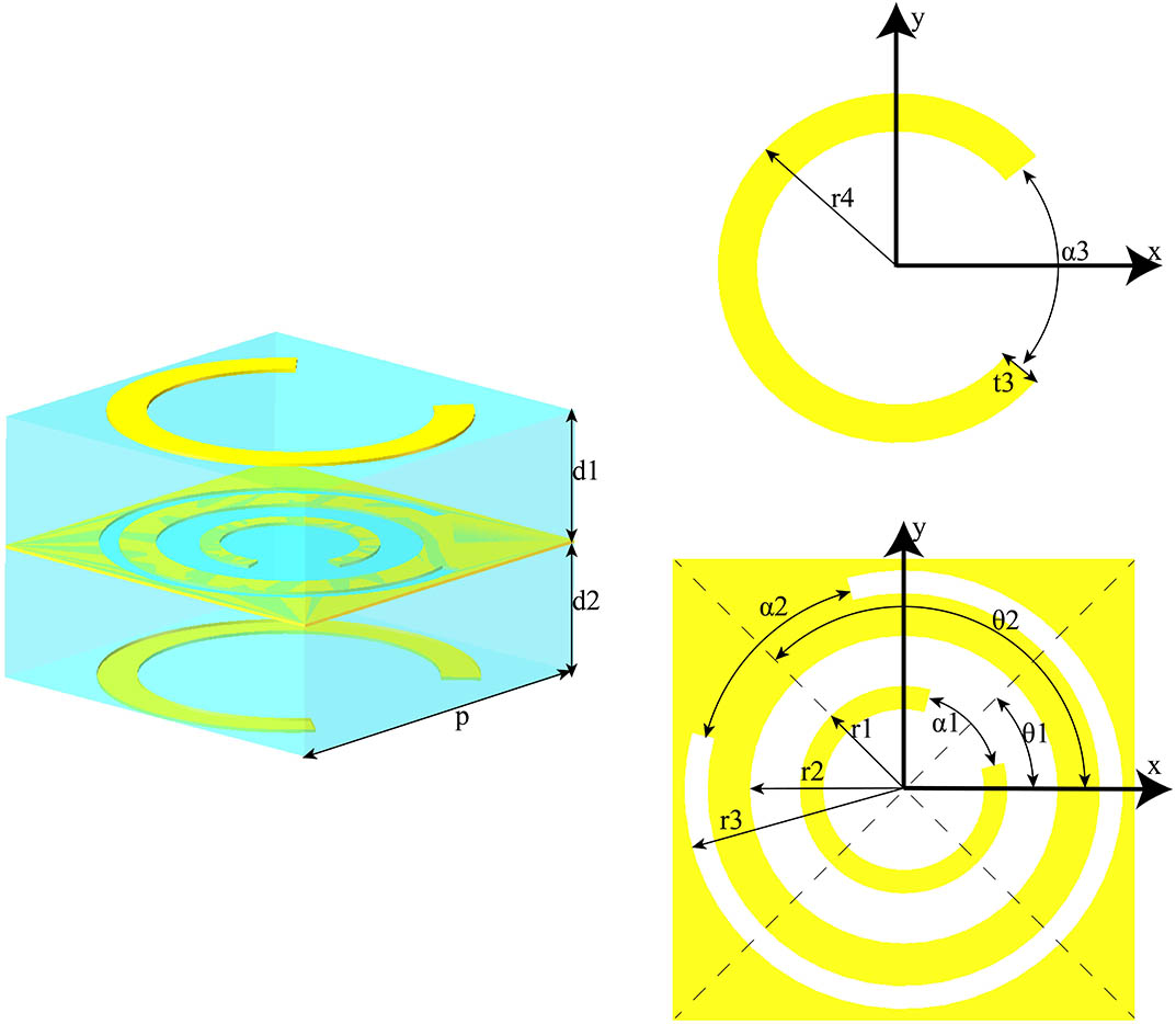
Figure 1 presents the schematic of the unit cell for the dual-wavelength microwave metasurface, which is composed of three metallic patterns printed on the two sides of the dielectric substrate of thickness with a permittivity of 4.6 and a loss tangent of 0.01. The front and back metallic patterns are two of the same CSRRs with split directions that are perpendicular to each other. The middle metallic layer is composed of a CSRR, a circular hole, and a CSSRR. The CSRR and CSSRR form a complementary structure to reduce the interaction between the CSSRR and CSRR due to their individual response characteristics. The geometries of the metallic C-shape pattern and CSSRR are also defined in Fig. 1.
Figure 1.Schematic of unit cell for the proposed metasurface. Left panel: 3D view of the basic element used in the simulation. Right panel: view of the top and bottom metallic layer (top panel) as well as the middle metallic layer (bottom panel).
The metasurface achieves the phase modulation by tuning the opening angle () and the orientation of the CSRR (CSSRR) () with respect to the axis. The radius of the circular hole is a significant factor because the size of the circular hole would effectively reduce the inevitable interference or coupling between the CSSRR and the CSRR[28]. The unit cell periodicity is optimized as 5.0 mm. According to the previous literature[30–32], the distances between the metallic layers may affect the efficiency of the device. Here, the geometric parameters of the metasurface are selected as , , , , , and .
To get the transmission phase and amplitude of the metasurface, numerical simulations are carried out based on Computer Simulation Technology (CST) Microwave Studio with the unit cell boundaries. Since the simulations are carried out at the microwave band, the metal can be taken as a perfect electric conductor (PEC). The incident waves are set as linear polarization, and we record the simulated phase and amplitude of cross-polarization transmission waves. From the simulation results shown in Figs. 2(a) and 2(b), it can be seen that the whole 360° phase shift can be approximated by a twelve-level phase modulation with 30° phase interval. The CSSRRs with different opening angles correspond to the different phases. In the design process, we select six appropriate CSSRRs with a 30° phase interval. Another six unit cells can be obtained just by rotating the orientation of previous six split-ring resonators about 90°, just like that done in Ref. [7]. The detailed geometrical parameters of CSSRR are presented in Table 1.
Variation of CSSRR
α2 (°)
θ2 (°)
Variation of CSRR
α1 (°)
θ1 (°)
1
165
−135
1
200
−135
2
150
−135
2
180
−135
3
120
−135
3
155
−135
4
85
−135
4
120
−135
5
45
−135
5
85
−135
6
10
−135
6
55
−135
7
165
−45
7
200
−45
8
150
−45
8
180
−45
9
120
−45
9
155
−45
10
85
−45
10
120
−45
11
45
−45
11
85
−45
12
10
−45
12
55
−45
Table 1. Opening Angle and Orientation of the Unit Cell
Figure 2.Simulated results of the twelve-level unit cells. (a) and (c) illustrate the phase response and transmission amplitude at 10 GHz under -polarized incidence, respectively. (b) and (d) illustrate the phase response and transmission amplitude at 20 GHz under -polarized incidence, respectively. (e) The polarization conversion ratio at 10 GHz under -polarized incidence. (f) The polarization conversion ratio at 20 GHz under -polarized incidence.
Note that the structure exhibits higher polarization conversion efficiency when the opening direction of the split-ring resonator is 45° with respect to the axis. Subsequently, we fix the orientation angle of the split-ring resonators as and for smaller amplitude fluctuation. Figure 2(a) presents the simulated phase responses at 10 GHz under -polarized incidence. We can see that the phase responses are almost completely independent with the variation of the CSRR. Figure 2(b) presents the simulated phase responses at 20 GHz under -polarization incident. Once again, the variation of the CSSRR has nearly no influence on the phase at 20 GHz, which is the fundamental reason that we can realize frequency-independent phase modulation at these frequencies. Furthermore, the transmission amplitudes of co-polarized () and cross-polarized () wave components at two wavelengths are shown in Figs. 2(c) and 2(d). The polarization conversion ratio is more than 90% at both frequencies.
To better understand the strategy to realize both dual-band and high conversion efficiency transmission for the proposed metasurface, the relationship between the incident and transmitted electric fields is described by the Jones’ matrix : where and are the co-polarized and cross-polarized transmission coefficients under -polarized incidence, and and are the co-polarized and cross-polarized transmission coefficients under -polarized incidence. According to the simulation results, we can see that and are nearly zero so that only the cross-polarized waves respond to the incident waves. The phases of cross-polarized waves under - and -polarized incidences are indicated as and , respectively, which could be tuned by changing the opening angle () and the orientation angle (). When the -polarized waves is incident, only at 20 GHz responds to the incident waves since the cross-polarized waves at 10 GHz barely exist, as shown in Fig. 3(a). Opposite situation is found for the case of the -polarized incidence. The strategy that different operating frequencies respond to the different polarizations could enhance the independence of the phase modulation in two wavelengths considering that the interactions between them are greatly reduced.
Figure 3.(a) illustrates the transmission amplitude at 10 GHz under -polarized incidence. (b) illustrates the transmission amplitude at 20 GHz under -polarized incidence.
Then, we proceed to design the array pattern of the metasurface after the unit cell is determined, aiming to generate different OAMs at different wavelengths. To generate the OAM with the metasurface under the plane wave irradiation, the phase distribution should be a total phase shift around one azimuthal cycle, according to the different topological charges. To be specific, the phase distribution on the metasurface can be expressed as[16]where is the topological charge, and is the azimuthal angle. The and represent the location of the unit cell. The and correspond to the incident waves of 10 and 20 GHz, respectively. The topological charges for different wavelengths are set as , and .
Considering the non-ideal planar wave generated by the near-field feeding source, a convergent phase can be considered to compensate the phase of the incident spherical wave. The spherical phase distribution is supposed to be written as where and are the wavelength and the focal length, respectively.
The focusing OAM beams can be generated by superimposing the helical phase and spherical phase. Subsequently, we design the corresponding phase distribution for 10 and 20 GHz, as shown in Figs. 4(a) and 4(b). The magnitude and phase of the electric-field distributions are calculated by the CST, which can be seen from Fig. 4. It is obvious that the zero-intensity presents in the center, which is generated by the phase singularity[33] of OAM beams, and can be observed in Figs. 4(c) and 4(d). The helical phase patterns shown in Figs. 4(e) and 4(f) exhibit the total phase shift for the OAM beam with topological charges and , which confirm the phase modulation capability of our structure at the near-field. There is a difference between the two wavelengths due to the introduction of spherical compensation phase.
Figure 4.Simulated results of generated OAM. (a) and (b) illustrate the phase distribution for 10 and 20 GHz, respectively. (c) and (e) illustrate the intensity pattern and phase pattern of the electric-field distributions at the position of under 10 GHz, respectively. (d) and (f) illustrate the intensity pattern and phase pattern of the electric-field distributions in near-field under 20 GHz at the position of , respectively.
In order to verify the phase modulation capability of our proposed metasurface structure in the far-field, we aim to design a deflector that can deflect the wavefront to the same direction at 10 and 20 GHz under normal incidence. According to the generalized Snell’s law, the refracted angle can be represented as under normal incident with and indicating the wavelength and the phase discontinuity along the axis. The and represent the case of 10 GHz with -polarized incidence and 20 GHz with -polarized incidence, respectively. It is obvious that the phase shift for 20 GHz should be double comparing that at 10 GHz. We selected the 12 CSSRRs with a 30° phase increment as a supercell for redirecting the incidence wave to 30° at 10 GHz. According to the above analysis, the six CSRRs with a 60° phase increment deflect the transmitted wave into 30° at 20 GHz.
After the selection of the unit cell, the full model was numerically simulated by CST with normal linear-polarized incidence. Figures 5(a) and 5(e) depict the simulated electric-field distribution () and 3D far-field patterns under the -polarized normal incidence at 20 GHz. Figures 5(b) and 5(f) depict the simulated electric-field distribution () and 3D far-field patterns under the -polarized normal incidence at 10 GHz. From the simulation results, we can observe that the deflected angles are 28° and 29° at 10 and 20 GHz, which are consistent with our design goals. Comparing the component and component of electric-field distribution at 20 GHz, we can clearly observe that the component of transmissive waves is nearly nonexistent; namely, most of the incident -polarization converts into the -polarization component, which shows the high conversion efficiency characteristics of the structure. A similar phenomenon can be observed from the simulated results at 10 GHz. In addition, the far-field simulated results also exhibit obvious deflecting performance.
Figure 5.Simulated results of deflector. (a) and (c) illustrate the simulated component and component of electric-field distribution under the -polarized normal incidence at 20 GHz, respectively. (b) and (d) illustrate the simulated component and component of electric-field distribution under the -polarized normal incidence at 20 GHz, respectively. (e) and (f) illustrate 3D far-field patterns under the -polarized normal incidence at 10 and 20 GHz, respectively.
The phase responses within the bands from 9 to 11 GHz and from 19 to 22 GHz shown in Figs. 6(a) and 6(b) are linearly varied with the frequency, which is mainly due to the designed unit cells operating at a broadband non-resonant regime. Subsequently, we simulated the full mode of the deflector at the frequency nearby the selected frequency to verify the achromatic property of our structure. The simulated component of the electric field at 19 and 24 GHz under -polarization incidence is presented in Figs. 6(c) and 6(e). The transmissive waves are deflected into 31° and 24° at 19 and 24 GHz, respectively. The transmissive waves are deflected into 35° and 26° at 9 and 11 GHz, respectively, as shown in Figs. 6(d) and 6(f). Note that the phase shift of each unit cell is linearly proportional to the frequency. Therefore, the phase gradient along the metasurface is invariant. According to the generalized refractive and reflective law in Refs. [6–8], it is not difficult to deduce that the deflection angle will change when the incident wavelength is different. That is to say, the proposed design cannot be utilized for broadband achromatic devices, which is in contrast with our previous work in Ref. [25]. Besides, by utilizing the optimizing algorithm, e.g., the particle swarm optimization algorithm, one can also construct broadband achromatic metasurfaces.
Figure 6.Simulated results of the deflector. (a) illustrates the phase shift under the -polarized normal incidence from 18 to 24 GHz, and the curves of different colors correspond to the different cells. (b) illustrates the phase shift under the -polarized normal incidence from 9 to 11 GHz. (c) and (e) illustrate the simulated component of electric-field distribution under the -polarized normal incidence at 19 and 24 GHz. (d) and (f) illustrate the simulated component of electric-field distribution under the -polarized normal incidence at 9 and 11 GHz.
In summary, the high-efficiency transmissive metasurface was demonstrated to independently modulate phase at two wavelengths. According to the simulated results, the conversion efficiency was above 90% for both wavelengths. The multiple OAM beams with different helixes were generated at the near-field to confirm the independent phase modulation capability. Subsequently, a deflector was designed to verify the deflection property of the structure. The simulated near-field and far-field results all showed good deflected performance at 10 and 20 GHz. The deflector at the frequency near the two pre-appointed frequencies also exhibited obvious deflected performance. Moreover, the proposed structure can integrate different functions in single device, which offers a new method for the multifunctional device in the future.