• Journal of Inorganic Materials
  • Vol. 35, Issue 10, 1177 (2020)
Futong SUN1、2, Aihu FENG2, Bingbing CHEN2, Yun YU2、*, and Hong YANG1、*
Author Affiliations
  • 1College of Chemistry and Materials Science, Shanghai Normal University, Shanghai 200234
  • 2Key Laboratory of Inorganic Coating Materials of Chinese Academy of Sciences, Shanghai Institute of Ceramics, Chinese Academy of Sciences, Shanghai 201899, China
  • show less
    DOI: 10.15541/jim20190615 Cite this Article
    Futong SUN, Aihu FENG, Bingbing CHEN, Yun YU, Hong YANG. Effect of Copper Pretreatment on Growth of Graphene Films by Chemical Vapor Deposition[J]. Journal of Inorganic Materials, 2020, 35(10): 1177 Copy Citation Text show less
    OM images of different copper substrates(a) Untreated copper substrate; (b) Hydrochloric acid etching treatment; (c) Hydrochloric acid etching and electrochemical polishing treatment; (d) Passivation paste etching; (e) Passivation paste etching and electrochemical polishing treatment
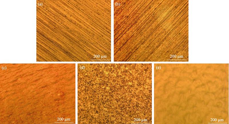
    1. OM images of different copper substrates(a) Untreated copper substrate; (b) Hydrochloric acid etching treatment; (c) Hydrochloric acid etching and electrochemical polishing treatment; (d) Passivation paste etching; (e) Passivation paste etching and electrochemical polishing treatment
    OM images of copper substrates electrochemical polished with different voltages and time(a1) 1.2 V/10 min; (a2) 1.2 V/20 min; (a3) 1.2 V/30 min; (a4) 1.2 V/40 min; (b1) 4 V/10 min; (b2) 4 V/20 min; (b3) 4 V/30 min; (b4) 4 V/40 min; (c1) 8 V/6 min; (c2) 8 V/8 min; (c3) 8 V/10 min; (c4) 8 V/12 min
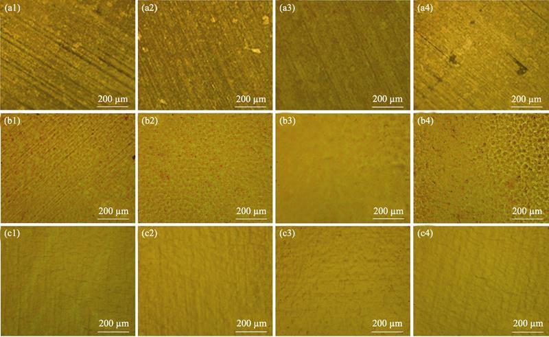
    2. OM images of copper substrates electrochemical polished with different voltages and time(a1) 1.2 V/10 min; (a2) 1.2 V/20 min; (a3) 1.2 V/30 min; (a4) 1.2 V/40 min; (b1) 4 V/10 min; (b2) 4 V/20 min; (b3) 4 V/30 min; (b4) 4 V/40 min; (c1) 8 V/6 min; (c2) 8 V/8 min; (c3) 8 V/10 min; (c4) 8 V/12 min
    OM images of copper substrates annealed at different temperatures for 30 min (a) 800 ℃; (b) 900 ℃; (c) 1000 ℃; (d) 1060 ℃
    3. OM images of copper substrates annealed at different temperatures for 30 min (a) 800 ℃; (b) 900 ℃; (c) 1000 ℃; (d) 1060 ℃
    OM images of copper substrates annealed at 1000 ℃ for different time (a) 0; (b) 30 min; (c) 90 min; (d) 120 min
    4. OM images of copper substrates annealed at 1000 ℃ for different time (a) 0; (b) 30 min; (c) 90 min; (d) 120 min
    SEM image of graphene sample
    5. SEM image of graphene sample
    Raman spectra of quartz substrate (a), graphene sample in gray area (b), and graphene sample in dark gray area (c)
    6. Raman spectra of quartz substrate (a), graphene sample in gray area (b), and graphene sample in dark gray area (c)
    AreaD band/cm-1G band/cm-12D band/cm-1ID/IGI2D/IG
    Gray area1354158126970.570.83
    Dark gray area1354159226840.261.29
    Table 1.

    Comparison of the Raman characteristic peak in different graphene areas

    Futong SUN, Aihu FENG, Bingbing CHEN, Yun YU, Hong YANG. Effect of Copper Pretreatment on Growth of Graphene Films by Chemical Vapor Deposition[J]. Journal of Inorganic Materials, 2020, 35(10): 1177
    Download Citation