1Institute of Integrated Microelectronic systems, College of Information Science and Electronic Engineering, Zhejiang University, Hangzhou 310027, China
2Zhejiang Lab, Hangzhou 310027, China
3United Microelectronics Center, Chongqing 404100, China
We demonstrate a single-chip silicon optical single sideband (OSSB) modulator composed of a radio frequency (RF) branch line coupler (BLC) and a silicon dual-parallel Mach–Zehnder modulator (DP-MZM). A co-design between the BLC and the DP-MZM is implemented to improve the sideband suppression ratio (SSR). The modulator has a modulation efficiency of and a 3 dB electro-optical (EO) bandwidth of 48.7 GHz. The BLC can generate a pair of RF signals with equal amplitudes and orthogonal phases at the optimal frequency of 21 GHz. We prove through theoretical calculation and experiment that, although the BLC’s performance in terms of power balance and phase orthogonality deteriorates in a wider frequency range, high SSRs can be realized by adjusting relevant bias phases of the DP-MZM. With this technique, the undesired sidebands are completely suppressed below the noise floor in the frequency range from 15 GHz to 30 GHz when the chip operates in the full carrier OSSB (FC-OSSB) mode. In addition, an SSR and an carrier suppression ratio (CSR) are demonstrated at 21 GHz in the suppressed carrier OSSB (SC-OSSB) mode.
1. INTRODUCTION
Optical single sideband (OSSB) modulation is an intensity modulation scheme that preserves one of the modulated sidebands and suppresses the other one. The anti-dispersion property of full carrier OSSB (FC-OSSB) modulation can be leveraged to overcome the power fading effect in various dispersive radio-over-fiber (RoF) links, such as multi-static radars and 5G/6G wireless communication systems [1,2]. Additionally, the optical frequency shifting function enabled by suppressed carrier OSSB (SC-OSSB) modulators has important applications in plenty of advanced photonics systems. For example, in microwave photonics systems, SC-OSSB modulators are used to implement frequency up/down conversions [3,4]. In light detection and ranging (Lidar) systems, SC-OSSB modulators can generate linearly chirped optical signals necessary for simultaneous velocity and distance detections [5–7]. The SC-OSSB modulator-based frequency shifter has also been used in a photonic quantum information processing system to erase the frequency distinguishability of non-degenerated photon pairs [8]. Moreover, OSSB modulators are used to reduce phase noise in a wireless THz-over-fiber system [9] and a narrow-linewidth light source [10]. Motivated by these applications, many advanced OSSB modulators have been demonstrated on different material platforms. Among them, OSSB modulators based on the silicon-on-insulator (SOI) platform are promising candidates thanks to the advantages of silicon photonics in CMOS compatibility, high integration density, etc. [11].
Bit rates of the state-of-the-art silicon digital modulators based on the carrier-depletion effect have reached 200 Gbit/s [12–16]. Inspired by the success of silicon digital modulators in high-speed optical interconnect systems, increasing research efforts are devoted to developing silicon modulators for analog optical links, e.g., high linearity modulators and OSSB modulators [17–22]. Most silicon OSSB modulators utilize the dual-parallel Mach–Zehnder modulator (DP-MZM) architecture [21,22]. This scheme requires two bias-tees to provide reverse biases for the PN junctions of two sub-MZMs, and a quadrature hybrid coupler (QHC) that generates a pair of radio frequency (RF) signals with equal amplitudes and quadrature phases to drive the two sub-MZMs. In most prior reports, these RF passive devices are implemented as discrete components. If these RF devices and the silicon DP-MZM can be monolithically integrated on the same chip, key performance metrics such as cost, footprint, reliability, parasitic, and link loss can be dramatically improved.
On-chip RF passive devices such as couplers, mixers, and antennas are quite prevalent in millimeter-wave integrated circuits (MMICs) [23–25]. However, there are very few attempts to monolithically integrate passive RF devices with silicon PICs due to compatibility issues in terms of processing flow and footprint. Important progress is made in Ref. [26], where a parallel dual-ring modulator (PDRM) and a QHC are integrated monolithically to enable an FC-OSSB modulator by leveraging IHP’s Photonic BiCMOS technology. The sideband suppression ratio (SSR) is 15 dB in the frequency range from 28 to 32 GHz. The lumped QHC in this work is formed by inductors and capacitors. However, integrated capacitors in MMICs usually suffer from poor accuracy. The typical capacitor tolerance of silicon integrated passive device (IPD) technology is within [27]. In contrast, branch line couplers (BLCs) consisting of coplanar waveguides (CPWs) or microstrip lines are more tolerable to manufacturing errors and, thus, are widely used to build RF power dividers or RF phase shifters in MMICs [28–31]. On the other hand, OSSB modulation usually requires cooperation between two sub-modulators. Therefore, the operation states of the two sub-modulators should be controlled precisely. Otherwise, the undesired sideband cannot be suppressed effectively. It is not easy to precisely control the resonance state of a microring modulator. In addition, OSSB modulators are widely used in microwave photonics systems, which usually use high optical powers to enhance their RF link gains. However, microring modulators suffer from strong optical nonlinearity at high optical power levels [32]. In contrast, MZMs have intrinsic advantages over microring modulators in terms of control simplicity and high-power handling ability and, thus, are well-suited for the OSSB modulators.
Sign up for Photonics Research TOC. Get the latest issue of Photonics Research delivered right to you!Sign up now
In this work, we monolithically integrate silicon DP-MZM and BLC by using the standard silicon photonics processing flow provided by the foundry and then realize a fully functional chip to implement FC-OSSB and SC-OSSB modulations. More importantly, we experimentally verify that, although the two RF outputs of the BLC exhibit considerable phase and amplitude errors as the frequency deviates from the optimum point, these errors can be corrected to some extent in the optical domain by adjusting the operation point of the DP-MZM. With this measure, undesired sidebands are completely suppressed in a wide frequency range from 15 to 30 GHz when the device operates in the FC-OSSB mode. Moreover, in the SC-OSSB mode, an SSR larger than 35 dB and a carrier suppression ratio (CSR) larger than 42 dB are achieved at the optimal frequency point of 21 GHz.
This paper is organized as follows. In Section 2, the device structure and the operation principle are explained. In Section 3, we first test the performances of the standalone DP-MZM and BLC units and then characterize the qualities of the FC-OSSB and SC-OSSB signals. Finally, we conclude the paper in Section 4.
2. DEVICE STRUCTURE AND OPERATION PRINCIPLE
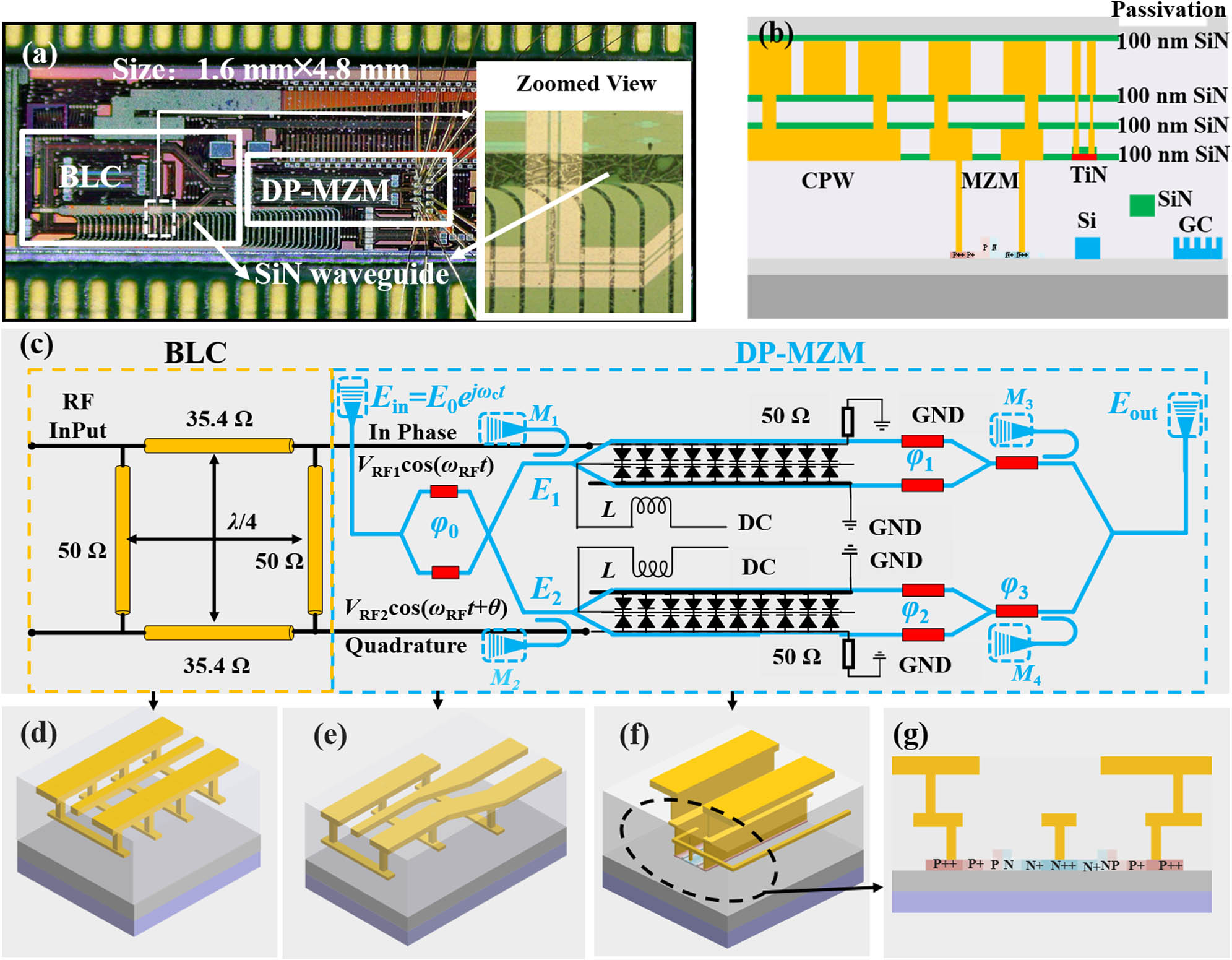
Figure 1(a) shows a microphotograph of the silicon OSSB modulator. The device is fabricated on a high-resistivity SOI wafer with a 2-μm-thick buried oxide (BOX) layer and a 220-nm-thick top silicon layer. The sizes of the BLC and DP-MZM are and , respectively, which result in an overall chip size of . The cross-sectional schematic view and the floorplan of the device are shown in Figs. 1(b) and 1(c), respectively. The three-dimensional structures of transmission line (TL) electrodes at various locations on the device are depicted in Figs. 1(d)–1(f).
Figure 1.(a) Microphotograph of the silicon OSSB modulation chip consisting of an RF BLC and a DP-MZM with adjustable optical power splitting ratio. (b) Cross section schematic diagram of the device, which includes the CPW with floating strips, carrier-depletion-based phase shifter, TiN heater, and grating coupler (GC). (c) Floorplan of the silicon OSSB modulation chip. (d) Three-dimensional (3D) diagram of the CPW transmission line with floating strips to suppress the slot-line mode. (e) 3D diagram of the reciprocal transition structure between CPW and CPS electrodes. (f) 3D diagram of the single-drive series push–pull MZM integrated with an inductive line. (g) Cross-sectional schematic diagram of the phase shifter.
The BLC is composed of four quarter-wavelength TLs with two different impedances of and [33]. It equally divides the input RF power to an in-phase port (I-port) and a quadrature port (Q-port) with a phase difference of 90°. Compared with the microstrip lines, CPWs are insensitive to substrate thickness and present low dispersion. Therefore, they are preferred by most reported on-chip BLCs [29–31]. We also utilize the CPW structure to build the BLC in this work. The signal electrode width, the ground electrode width, and the gap between the signal and ground electrodes are 17.4 μm, 50 μm, and 6.3 μm for the two CPWs, respectively. The values of these parameters are 24.6 μm, 50 μm, and 2.7 μm for the two CPWs. As shown in Figs. 1(d) and 1(e), there are metallic floating strips with a pitch of 200 μm beneath the CPWs. They are used to equalize the potentials of two ground electrodes so that the detrimental slot-line mode excited at discontinuities of the signal lines is suppressed [34]. The RF outputs of and ports are fed to two sub-MZMs through transition structures between the CPW and coplanar stripline (CPS), as shown in Fig. 1(e) [35,36]. According to the foundry’s design rule, in the areas where there are SiN waveguides or grating couplers (GCs) under the CPW, the etch stop nitride layers are selectively removed to avoid the coupling loss, as shown in the zoomed view of Figs. 1(a) and 1(b). The discontinuity of material stacking together with the raised dielectric surface roughness caused by the removal of etch stop nitride layers inevitably changes the RF propagation characteristic of the CPW and then worsens the performance of the BLC.
The single-drive series push–pull configuration is utilized by the two sub-MZMs. A thermo-optical (TO) switch before the two sub-MZMs controls the optical power splitting ratio between them. A three-dimensional diagram and a cross-sectional view of the two modulation arms are shown in Figs. 1(f) and 1(g), respectively. The ridge waveguide width and the slab thickness are 500 nm and 90 nm, respectively. A lateral PN junction is embedded in each arm to implement the high-speed electro-optical (EO) modulation. The junction is formed by lightly doped and regions at the center of the ridge waveguide. Intermediately doped and regions are 400 nm away from the waveguide center so as to reduce the series resistance of the PN junction without introducing additional optical loss. Heavily doped and regions are located 1200 nm away from waveguide center to enable ohmic contacts. The nominal peak doping concentrations are , , , , , and for , , , , , and regions, respectively. As shown in Fig. 1(g), two PN junctions of the sub-MZM are connected in series with reversed polarities. A CPS traveling wave electrode drives the two PN junctions simultaneously. The signal and ground lines of the CPS electrode are 50 μm wide and spaced by 35 μm. To avoid RF reflection, an on-chip resistor made of TiN film is placed at the end of the CPS electrode. Considering the trade-off between the modulation depth and the speed, the phase shifter length is chosen to be 1.5 mm. The DC bias is connected to the common region of the two PN junctions through a 10-μm-wide inductive line. As shown in Figs. 1(c) and 1(f), TiN heaters with identical dimensions of μμ are incorporated at all modulation arms so as to tune the operation state of the DP-MZM. Their power consumptions are measured to be 20 mW per phase shift. Four optical power monitors consisting of a 10%/90% directional coupler and a fiber GC are used to probe the operation state of the device.
Non-ideal factors of the practical device deteriorate the OSSB signal quality, including the limited extinction ratios (ERs) of the two sub-MZMs due to the uneven outputs of practical multimode interferometers, power imbalance, and phase non-orthogonality between the two RF outputs of the BLC [21]. As will be experimentally verified in Section 3, the ERs of fabricated silicon MZMs are larger than 30 dB, so they are not the major performance bottleneck. As a result, in the following context of this section, we only theoretically analyze the influence of BLC’s imperfect output characteristic on OSSB modulation,
As shown in Fig. 1(c), the on-chip incident optical field is written as , where and denote the amplitude and the angular frequency of the optical field, respectively. The two RF outputs of the BLC are and , where , , and represent amplitudes, angular frequency, and phase difference of the two RF signals, respectively. Two output optical fields of the optical switch are determined by the relative phase between the two arms, and they are calculated as and . The ratio between input optical powers of the two sub-MZMs then is . Under these symbols, the output optical field of the OSSB modulator is expressed by Eq. (1), where are static bias phases of the two sub-MZMs and the parent-MZM. In order to simplify the discussion, the free carrier absorption (FCA) is not taken into account in Eq. (1). However, our previous analysis in Ref. [21] indicates that the validity of the model is not affected much by this simplification. By expanding Eq. (1) into the Jacobi–Anger series, we obtain analytical expressions of all modulation sidebands, which are not listed here for brevity. According to the analytic formulas of two first-order sidebands, it is easy to deduce the necessary conditions of FC-OSSB modulation, which are written as
Here , , , , and denotes the Bessel function of the first kind.
The two expressions in Eq. (2) imply that, if the output characteristics of the BLC are non-ideal (i.e., , ), it is still possible to completely suppress one of the first-order sidebands by tuning the two TO phase shifters (i.e., and ). However, the power of the retained first-order sideband in this case would decay to some degree. This point is illustrated by the calculation result in Fig. 2, where the power of the retained first-order sideband relative to its peak value is plotted as a function of the amplitude ratio and the phase difference between the two RF outputs of the BLC. In this calculation, values of and are determined by Eq. (2) so that the other first-order sideband is fully eliminated. Assuming that the maximum acceptable power attenuation is 10 dB, i.e., , the amplitude imbalance should not be smaller than , i.e., , and the phase difference between the RF driving signal pair should not deviate from by more than , i.e., . In Fig. 2, we highlight the contour line where the power penalty of the retained sideband is 10 dB. In the region surrounded by this contour line, the errors of the RF output can be corrected by the silicon DP-MZM with an acceptable power penalty.
Figure 2.Power attenuation of the retained sideband versus the amplitude imbalance and the phase difference between the RF outputs of and ports.
Before the OSSB modulation measurement, we test the performances of the DP-MZM and the BLC. The overall on-chip insertion loss (IL) of the DP-MZM is measured to be . It can be broken down to a loss of the sub-MZM, a loss of the optical switch, a loss induced by four optical power monitors, a loss of the optical combiner, and a loss of a 0.7-cm-long routing waveguide. The modulation efficiency is quantified with a reference imbalanced MZM structure with 1.5-mm-long phase shifters. Its optical transmission spectra under different DC reversed bias voltages are shown in Fig. 3(a). The measured ERs are larger than 30 dB, so there is a good power balance between the two modulation arms. The corresponding is about under 2 V bias. With a Keysight 67 GHz lightwave component analyzer (LCA, Keysight N4373D, N5247A), we characterize the small signal responses of the DP-MZM and plot the results in Fig. 3(b). The measured 3 dB bandwidth is 48.7 GHz. The electro-electro (EE) parameter is below in the frequency range from 10 MHz to 67 GHz, which suggests that the impedance matching condition needs to be improved in the future.
Figure 3.(a) Optical transmission spectra of the imbalanced reference MZM under different reversed bias voltages. The coupling losses of two grating couplers have been normalized. (b) Measured EE and EO parameters of the MZM. (c) Measured EO crosstalk between the two sub-MZMs with a pitch of 300 μm.
If silicon MZMs are in proximity, it is necessary to investigate the EO crosstalk between them [37]. When testing the EO crosstalk, we switch all incident light to sub-MZM1, as shown in the inset of Fig. 3(c). The RF driving signal is then fed to sub-MZM2 through RF input port 3. A part of the RF signal is coupled to the CPS electrode of sub-MZM1 and then modulates the optical wave propagating inside sub-MZM1. The EO crosstalk is defined as the EO response of the victim sub-MZM1 induced by the RF signal applied to the aggressor sub-MZM2. It is calculated as , where and are the EO responses of sub-MZM1 when the RF signal is fed to ports 1 and 3, respectively. The measured EO crosstalk shown in Fig. 3(c) is below , which suggests that the 300 μm pitch between the two sub-MZMs is sufficient for RF isolation.
After testing the silicon DP-MZM, we measure the performance of the BLC. Simulated and measured frequency responses of and ports of the BLC are shown in Figs. 4(a) and 4(b), respectively. Compared with the simulation result (solid lines), the measured performance of BLC in Fig. 4(b) degrades considerably in terms of additional loss, phase orthogonality, and power uniformity. As shown in Fig. 1(a), there are plenty of SiN waveguides beneath the quarter-wavelength TLs of the BLC so as to make full use of the valuable chip area. The discrepancy between simulation and measurement results can be partially attributed to the non-homogeneity in the surrounding circumstances of the BLC and the surface roughness of the practical metal layer. We performed high-frequency simulations to quantify their impacts. The simulation results indicate that the metal surface roughness has a more pronounced impact on the BLC’s performance than the SiN waveguides. The short dashed lines in Fig. 4(a) show the effect of introducing the Huary model to assess the metal surface roughness [38,39]. It is found that the IL, the power uniformity, and the phase orthogonality of the BLC deteriorate to some extent. After considering the meal surface roughness, the simulation results fit the measurements in Fig. 4(b) better.
Figure 4.(a) Simulated and (b) measured RF output characteristics of the and ports of the BLC.
In Section 2, we have proved theoretically that the power of the retained first-order sideband reaches its peak value when the RF outputs of and ports are equal in amplitude and quadrature in phase. Otherwise, although the unwanted first-order sideband can still be suppressed by adjusting the two TO phase shifters, the retained first-order sideband would decay due to the power and phase detuning of the RF driving signal pair. In Fig. 4(b), we can find an optimal frequency point of 21 GHz. Although the two RF outputs are weaker than expected at this frequency, the power uniformity and phase orthogonality conditions are well satisfied. Therefore, we expect the retained first-order sideband to present the strongest power at this frequency.
In the OSSB modulation measurement, an RF generator (Keysight E8267D) provides a 20 dBm RF driving signal whose frequency is swept from 15 GHz to 30 GHz. The RF signal is fed to the device by a ground-signal-ground (GSG) probe. The two sub-MZMs are biased at the quadrature and the null points to implement the FC-OSSB and the SC-OSSB modulations, respectively. In order to obtain high SSRs, we adjust the thermal tuning power of the optical switch as well as that of the parent-MZM. The measured optical spectra of OSSB signals with and without carriers are plotted in Figs. 5(a) and 5(b), respectively. In the FC-OSSB mode, the undesired sidebands are well suppressed below the noise floor of at all testing frequencies. The practical SSRs, therefore, are larger than 20 dB. In the SC-OSSB mode, the power of the carrier falls by 42 dB as compared with the FC-SSB mode. The worst SSR of 17 dB occurs at 28 GHz. The best and worst ERs between the carrier and the retained sideband are 19.7 dB at 21 GHz and 9.4 dB at 30 GHz, respectively. The practical values of are plotted in Fig. 5(c). We note that the remaining sidebands in both Figs. 5(a) and 5(b) reach their peak powers at 21 GHz. This phenomenon is in line with the measurement result in Fig. 4(b), where the BLC offers the best performance at this frequency.
Figure 5.Output spectra of the OSSB modulator with a resolution of 0.02 nm in (a) the FC-OSSB mode and (b) the SC-OSSB mode. (c) Practical values of to enable high SSRs at different frequencies.
As a proof-of-concept demonstration, a passive RF BLC and an active silicon DP-MZM are monolithically integrated to realize a fully functional OSSB modulator chip. Although the performance of the BLC is constrained by the imperfect processing control, we still obtain high SSRs by adjusting the optical splitting ratio of DP-MZM. The measured SSRs in the FC-OSSB modulation mode are larger than 20 dB in the frequency range from 15 GHz to 30 GHz, while the measured SSR and CSR in the SC-OSSB modulation mode are better than 35 dB and 42 dB at 21 GHz, respectively.
Efforts can be made to further improve the performance of the device in the following aspects in the future. First, little attention is paid to the conversion efficiency, i.e., , when we set the phase shifter length. Considering the intrinsic trade-off between the IL and the modulation depth of the carrier-depletion-based phase shifter, the optimal phase shifter length with maximized conversion efficiency is . Our calculation indicates that the sideband power is at this length given that the incident optical power is 0 dBm and the RF signal amplitudes are , respectively. Through a proper TW electrode design, the bandwidth can still reach for this length [40]. Second, the BLC takes up around 54% of the total footprint. Therefore, the miniaturization of the BLC is recommended. Fortunately, there are plenty of mature schemes to reduce the BLC size in MMICs, such as line loading and line folding structures [29,30]. For example, the footprint of the BLC shrinks by 73% in Ref. [29] after using the elevated-center CPW structure. Third, the signal integrity between BLC and DP-MZM can be improved by further optimizing the reciprocal transition structure between CPS and CPW.
In conclusion, we integrate typical photonic device and RF passive device on SOI substrate and prove that the easy tunability of the silicon PIC can be leveraged to alleviate the performance degradation of the practical RF passive device. In other words, imperfect photonics and RF components on the chip can work collaboratively to achieve a good overall performance. We believe that the methodology of this work helps to elevate the integration level of microwave photonics circuits.
Acknowledgment
Acknowledgment. The authors thank Dr. Bing Wei, Training Platform of Information and Microelectronic Engineering in Polytechnic Institute of Zhejiang University.
[2] C. Browning, X. Ouyang, D. Dass, G. Talli, P. Townsend. Orthogonal chirp-division multiplexing for performance enhanced optical/millimeter-wave 5G/6G communications. Optical Fiber Communication Conference (OFC), W1J.3(2021).
[12] E. Timurdogan, Z. Su, R. Shiue, M. J. Byrd, C. V. Poulton, K. Jabon, C. DeRose, B. R. Moss, E. S. Hosseini, I. Duzevik, M. Whitson, R. P. Millman, D. A. Atlas, M. R. Watts. 400G silicon photonics integrated circuit transceiver chipsets for CPO, OBO, and pluggable modules. Optical Fiber Communication Conference (OFC), T3H.2(2020).
[16] M. Sakib, P. Liao, C. Ma, R. Kumar, D. Huang, G. Su, X. Wu, S. Fathololoumi, H. Rong. A high-speed micro-ring modulator for next generation energy-efficient optical networks beyond 100 Gbaud. Conference on Lasers and Electro-Optics, SF1C.3(2021).
[22] A. Kodigala, M. Gehl, C. T. DeRose, D. Hood, A. T. Pomerene, C. Dallo, D. Trotter, P. Moore, A. L. Starbuck, J. Lee, G. Biedermann, A. L. Lentine. Silicon photonic single-sideband generation with dual-parallel Mach-Zehnder modulators. Conference on Lasers and Electro-Optics (CLEO), STh4N.6(2019).
[27] K. R. Shin, K. Eilert, N. Mellen. Compact size cellular/GSM band pass filter with high resistivity thin film silicon integrated passive device (IPD) technology. IEEE MTT-S International Microwave Symposium (IMS), 1-4(2016).
[30] S. Shopov, R. E. Amaya, J. W. M. Rogers, C. Plett. High-performance reduced-size 70–80 GHz CMOS branch-line hybrid using CPW and CPWG guided-wave structures. IEEE/MTT-S International Microwave Symposium Digest, 1-3(2012).
[39] P. G. Huray, O. Oluwafemi, J. Loyer, E. Bogatin, X. Ye. Impact of copper surface texture on loss: a model that works. DesignCon, 1, 462-483(2010).