
Hailong Han, Hao Li, Lixing You, Xiaoping Liu. Fabrication and characterization of on-chip silicon spherical-like microcavities with high Q-factors[J]. Chinese Optics Letters, 2022, 20(11): 111301
- Chinese Optics Letters
- Vol. 20, Issue 11, 111301 (2022)
Abstract
1. Introduction
Optical microcavities have attracted considerable attention and played an essential role in on-chip classic and quantum information processing during the past decades[
We propose fabricating on-chip silicon spherical microcavities by heating a large silicon pillar on a silicon pedestal or a mushroom-like silicon structure on a silicon-on-insulator (SOI) substrate with a laser under atmospheric pressure and at room temperature. Different etching processes are used in our experiment to prepare these unique structures; a careful direct laser-heating step with proper influence then reshapes these mushroom-like structures into spherical microcavities by reflowing the whole structure. The exact shape and morphology of the prepared silicon spherical microcavities are characterized using a scanning electron microscope (SEM) and an atomic force microscope (AFM). Optical whispering gallery modes (WGMs) of these spherical microcavities are tested using a tapered-fiber coupling system, in which a loaded-Q on the order of is demonstrated.
2. Experiment
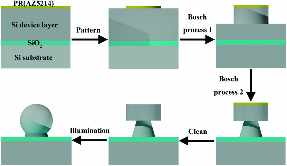
Our experiment fabricated silicon spherical microcavities on a commercial SOI wafer with a 16-µm-thick device layer and a 2-µm-thick buried oxide. The device layer is n-type silicon with orientation (100) and resistance of 10–20 Ω·cm. Instead of using a single silicon pillar, a mushroom-like structure, where a silicon pillar sits on a narrow pedestal, as shown in Fig. 1, is used to fabricate a spherical microcavity by reflowing. The reason for not using a single pillar is that reflowing such a structure in experiments makes it difficult to form a spherical shape due to silicon’s low surface tension. Two-step Bosch processes with different process parameters are adopted in a sequence to prepare the mushroom-like structure. A Bosch process requires two kinds of gases, where the gas does the etching while gas deposits a passivation layer to inhibit the already etched and exposed sidewall. A very deep silicon etching could be achieved periodically by alternating these two gases. The etched sidewall is usually not perfectly vertical microscopically, but instead, it is curvy because of the tendency of isotropic etching and periodic along the vertical etching direction because of the periodic alternation of two gases. Usually, with a considerable period, the sidewall becomes increasingly curvy. This effect is exploited to make a unique mushroom-like silicon structure by tuning different time ratios between etching and passivation.
Sign up for Chinese Optics Letters TOC. Get the latest issue of Chinese Optics Letters delivered right to you!Sign up now
![]()
Figure 1.Flowchart of the fabrication processes.
Detailed step-by-step fabrication processes are presented in Fig. 1. First, the commercial SOI wafer mentioned above is cleaned and spin-coated with a layer of photoresist (AZ5214) about 1.5 µm thick and then patterned with a mask-less photolithography system (SF-100, Intelligent). Second, after development, the first Bosch process is performed in the HSE200s Deep Silicon Etcher. The top part of a mushroom-like structure, a silicon pillar, forms after 60 cycles of Bosch processes. The size of this pillar primarily determines the size of the spherical microcavity prepared later by laser reflowing. Third, another Bosch process is used to prepare the pedestal of the mushroom-like structure by first depositing a thick passivation layer on the already formed silicon pillar to prevent it from being further etched. Next, the pillar is undercut to create a narrow pedestal via a relatively long etching time to complete the mushroom-like structure. The main parameters of two different Bosch processes are listed in Table 1. Finally, a direct laser-heating step with an adequately controlled influence reshapes the mushroom-like structure to a more-or-less spherical silicon microcavity with the help of silicon surface tension in its liquid state during heating. An optical laser beam with a wavelength of 532 nm and an emission power of 5 W (Coherent Verdi V18), which silicon strongly absorbs, is focused onto the fabricated structure with an estimated optical intensity of . A programmable shutter is used to precisely control the laser illumination time. After several rounds of optimization, a suitable illumination time for our structure is determined to be about 0.005 s. The energy density imposed on this structure is estimated to be .
| 1st Bosch Process | 2nd Bosch Process | ||
|---|---|---|---|
| Passivation time/cycle | Etching time/cycle | Passivation time/cycle | Etching time/cycle |
| 0.8 s | 1.7 s | 7 s | 24.5 s |
| Number of cycles: 60 | Number of cycles: 1 | ||
Table 1. Main Parameters of Bosch Processes
3. Results and Discussion
The exact shapes of our fabricated on-chip samples before and after 532 nm laser illumination are characterized using SEM and shown in Fig. 2. A side review of an as-etched sample shown in Fig. 2(a) reveals the mushroom-like structure. Further investigations show that this pillar has a diameter of about 15 µm and a height of about 6.5 µm. Figures 2(b) and 2(c) show the silicon structure’s front and top views after laser illumination. The newly formed structure has a nearly spherical shape except for the north pole region, which has a noticeable bump. A strong correlation is found between the location of this bump and the moving direction of the blade inside the shutter during the closing of the shutter. It is thus suspected that the bump is the last part of the silicon spherical-like structure to solidify during the sudden cooling down caused by the laser illumination being blocked by the shutter. The low surface tension of silicon cannot completely smooth the surface before the structure solidifies. The low surface tension is also responsible for the unsuccessful attempts of forming a silicon sphere when only a silicon pillar without a pedestal is used for laser heating and reflow. It is found experimentally in this case that only a half-sphere could be formed. However, without a clearly defined equator, this half-sphere does not support high- optical WGMs. To solve this issue, the current mushroom-like structure is developed, and, with it, the formed spherical-like silicon structure has an exposed equator zone with a diameter measured to be close to 15 µm. Figure 2(d) shows the zoom-in SEM view of the details of the surface of the sphere-like silicon microcavity near the equator region. The overall surface Q is excellent, judging from its surface smoothness.
![]()
Figure 2.SEM images of our prepared sample. (a) Side view before laser illumination, (b) and (c) side view and top view after laser illumination, and (d) zoom-in view of the edge after laser illumination.
To further investigate its surface Q, AFM is utilized to observe the surface morphology of this fabricated silicon sphere-like microcavity, and a representative AFM image for regions near the equator is shown in Fig. 3. The root-mean-square (RMS) roughness, calculated from the measured data, is only about 0.6 nm. As a comparison, the surface roughness of the commercially available polished Si substrate is about 0.2 nm[
![]()
Figure 3.AFM image of the fabricated silicon spherical microcavity.
The resonance spectrum and -factor of our silicon sphere-like microcavities’ modes are characterized via an evanescent coupling method using an optical fiber taper[
Figure 4(a) shows a section for the wavelength range from 1515 to 1525 nm. The resonances of the WGMs of the silicon sphere-like microcavity are observed as the corresponding Lorentzian dip families in the shown spectrum. The -factor is defined as the ratio of the energy stored in the oscillating cavity to the energy dissipated per cycle by damping processes[
![]()
Figure 4.(a) Transmission spectrum of the microcavity coupled with the fiber taper from 1515 to 1525 nm; (b) the Lorentzian fit (solid red line) of the measured spectrum around the resonant wavelength at 1519.6 nm (solid black line), showing a Q-factor of 3.5 × 10⁵.
4. Conclusions
In conclusion, we have proposed and demonstrated a method to fabricate high--factor on-chip silicon sphere-like microcavities by laser heating a particular mushroom-like silicon structure. To fabricate such structures, two different Bosch processes are developed. With the illumination of an intense 532 nm laser beam, this particular structure can be melted and reshaped into a silicon sphere-like microcavity, which has a clear exposed equator that can be used to exploit WGMs. The advantage of this method is apparent in that it allows for fabricating relatively large microcavities and, importantly, gives rise to a minimal surface RMS roughness, only about 0.6 nm. This, in turn, leads to WGM resonances with instrumentally limited loaded -factors above . We believe that this fabrication method may open new avenues for cost-effective large-area processing of complex three-dimensional (3D) optical cavity structures and promises great potential in nonlinear light–matter interactions.
References
[1] K. J. Vahala. Optical microcavities. Nature, 424, 839(2003).
[2] J. Ward, O. Benson. WGM microresonators: sensing, lasing and fundamental optics with microspheres. Laser Photonics Rev., 5, 553(2011).
[3] M. Cai, O. Painter, K. J. Vahala, P. C. Sercel. Fiber-coupled microsphere laser. Opt. Lett., 25, 1430(2000).
[4] T. Bilici, S. Isci, A. Kurt, A. Serpengüzel. Microsphere-based channel dropping filter with an integrated photodetector. IEEE Photon. Tech. Lett., 16, 476(2004).
[5] M. Cai, G. Hunziker, K. J. Vahala. Fiber-optic add-drop device based on a silica microsphere-whispering gallery mode system. IEEE Photon. Technol. Lett., 11, 686(1999).
[6] H. C. Tapalian, J. P. Laine, P. A. Lane. Thermooptical switches using coated microsphere resonators. IEEE Photon. Technol. Lett., 14, 1118(2002).
[7] I. Teraoka, S. Arnold, F. Vollmer. Perturbation approach to resonance shifts of whispering-gallery modes in a dielectric microsphere as a probe of a surrounding medium. J. Opt. Soc. Am. B, 20, 1937(2003).
[8] J. P. Laine, C. Tapalian, B. Little, H. Haus. Acceleration sensor based on high-Q optical microsphere resonator and pedestal antiresonant reflecting waveguide coupler. Sens. Actuators A Phys., 93, 1(2001).
[9] A. B. Matsko, A. A. Savchenkov, V. S. Ilchenko, L. Maleki. Optical gyroscope with whispering gallery mode optical cavities. Opt. Commun., 233, 107(2004).
[10] H. Lee, T. Chen, J. Li, K. Y. Yang, S. Jeon, O. Painter, K. J. Vahala. Chemically etched ultrahigh-Q wedge-resonator on a silicon chip. Nat. Photonics, 6, 369(2012).
[11] M. L. Gorodetsky, A. A. Savchenkov, V. S. Ilchenko. Ultimate Q of optical microsphere resonators. Opt. Lett., 21, 453(1996).
[12] D. K. Armani, T. J. Kippenberg, S. M. Spillane, K. J. Vahala. Ultra-high-Q toroid microcavity on a chip. Nature, 421, 925(2003).
[13] R. Schilling, H. Schütz, A. H. Ghadimi, V. Sudhir, D. J. Wilson, T. J. Kippenberg. Near-field integration of a SiN nanobeam and a SiO2 microcavity for Heisenberg-limited displacement sensing. Phys. Rev. Appl., 5, 054019(2016).
[14] M. Pöllinger, D. O’Shea, F. Warken, A. Rauschenbeutel. Ultrahigh-Q tunable whispering-gallery-mode microresonator. Phys. Rev. Lett., 103, 053901(2009).
[15] S. I. Shopova, H. Zhou, X. Fan, P. Zhang. Optofluidic ring resonator based dye laser. Appl. Phys. Lett., 90, 221101(2007).
[16] Y. Yang, S. Saurabh, J. M. Ward, S. N. Chormaic. High-Q, ultrathin-walled microbubble resonator for aerostatic pressure sensing. Opt. Express, 24, 294(2016).
[17] R. Shankar, R. Leijssen, I. Bulu, M. Lončar. Mid-infrared photonic crystal cavities in silicon. Opt. Express, 19, 5579(2011).
[18] C. Reimer, M. Nedeljkovic, D. J. M. Stothard, M. O. S. Esnault, C. Reardon, L. O’Faolain, M. Dunn, G. Z. Mashanovich, T. F. Krauss. Mid-infrared photonic crystal waveguides in silicon. Opt. Express, 20, 29361(2012).
[19] G. P. Agrawal. Nonlinear Fiber Optics(1995).
[20] S. A. Miller, M. Yu, X. Ji, A. G. Griffith, J. Cardenas, A. L. Gaeta, M. Lipson. Low-loss silicon platform for broadband mid-infrared photonics. Optica, 4, 707(2017).
[21] K. Srinivasan, H. X. Miao, M. T. Rakher, M. Davanco, V. Aksyuk. Optomechanical transduction of an integrated silicon cantilever probe using a microdisk resonator. Nano Lett., 11, 791(2011).
[22] M. Garín, R. Fenollosa, R. Alcubilla, L. Shi, L. Marsal, F. Meseguer. All-silicon spherical-Mie-resonator photodiode with spectral response in the infrared region. Nat. Commun., 5, 3440(2014).
[23] R. Fenollosa, F. Meseguer, M. Tymczenko. Silicon colloids: from microcavities to photonic sponges. Adv. Mater., 20, 95(2008).
[24] S. C. Hung, S. C. Shiu, C. H. Chao, C. F. Lin. Fabrication of crystalline Si spheres with atomic-scale surface smoothness using homogenized KrF excimer laser reformation system. J. Vac. Sci. Technol. B, 27, 1156(2009).
[25] J. Wu, Y. Huang, Y. Lin, Q. Li, J. Huang, T. Wu, C. Guo. Whispering gallery modes from silicon microsphere in C-band. IEEE Photon. Technol. Lett., 27, 1993(2015).
[26] X. Li, A. Pyatenko, Y. Shimizu, H. Wang, K. Koga, N. Koshizaki. Fabrication of crystalline silicon spheres by selective laser heating in liquid medium. Langmuir, 27, 5076(2011).
[27] J. Takahashi, T. Tsuchizawa, T. Watanabe, S. Itabashi. Oxidation-induced improvement in the sidewall morphology and cross-sectional profile of silicon wire waveguides. J. Vac. Sci. Technol. B, 22, 2522(2004).
[28] D. K. Sparacin, S. J. Spector, L. C. Kimerling. Silicon waveguide sidewall smoothing by wet chemical oxidation. J. Light. Technol., 23, 2455(2005).
[29] H. Kuribayashi, R. Hiruta, R. Shimizu, K. Sudoh, H. Iwasaki. Shape transformation of silicon trenches during hydrogen annealing. J. Vac. Sci. Technol. A, 21, 1279(2003).
[30] H. Hara, Y. Sano, K. Arima, K. Yagi, J. Murata, A. Kubota, H. Mimura, K. Yamauchi. Catalyst-referred etching of silicon. Sci. Technol. Adv. Mater., 8, 162(2007).
[31] J. C. Knight, G. Cheung, F. Jacques, T. A. Birks. Phase-matched excitation of whispering gallery modes by a fiber taper. Opt. Lett., 22, 1129(1997).
[32] Y. Chen, Y. Yin, L. Ma, O. G. Schmidt. Recent progress on optoplasmonic whispering-gallery-mode microcavities. Adv. Opt. Mater., 9, 2100143(2021).

Set citation alerts for the article
Please enter your email address
© Copyright 2018-2021 | Chinese Laser Press. All Rights Reserved 沪ICP备15018463号-20