• Chinese Optics Letters
  • Vol. 19, Issue 7, 071403 (2021)
Cheng Yin1, Xuefen Kan1, Kun Guo2, Tao Wang2, Jiangming Xu2, Qingbang Han1, Jian Wu2、*, and Zhuangqi Cao3
Author Affiliations
  • 1College of Internet of Things Engineering, Hohai University, Changzhou 213022, China
  • 2College of Advanced Interdisciplinary Studies, National University of Defense Technology, Changsha 410073, China
  • 3Department of Physics and Astronomy, Shanghai Jiao Tong University, Shanghai 200240, China
  • show less
    DOI: 10.3788/COL202119.071403 Cite this Article Set citation alerts
    Cheng Yin, Xuefen Kan, Kun Guo, Tao Wang, Jiangming Xu, Qingbang Han, Jian Wu, Zhuangqi Cao. Highly twisted M-line of a vortex beam due to the coupling of ultrahigh-order modes[J]. Chinese Optics Letters, 2021, 19(7): 071403 Copy Citation Text show less

    Abstract

    In modern optics, particular interest is devoted to the phase singularities that yield complicated and twisted phase structures by photons carrying optical angular momentum. In this paper, the traditional M-line method is applied to a vortex beam (VB) by a symmetric metal cladding waveguide chip, which can host numerous oscillating guided modes via free space coupling. These ultrahigh-order modes (UOMs) result in high angular resolution due to the high finesse of the resonant chip. Experiments show that the reflected pattern of a VB can be divided into a series of inner and outer rings, whilst both of them are highly distorted by the M-lines due to the UOMs’ leakage. Taking the distribution of the energy flux into account, a simple ray-optics-based model is proposed to simulate the reflected pattern by calculating the local incident angle over the cross section of the beam. The theoretical simulations fit well with the experimental results, and the proposed scheme may enable new applications in imaging and sensing of complicated phase structures.

    1. Introduction

    It is well known that a light beam with a phase singularity nested in its wave front carries an orbital angular momentum (OAM) equivalent to l per photon[1]. Now, there is considerable interest in these unique properties arising from the special phase structures[2]. The vortex beam (VB) has many applications in optical manipulation[3], optical communications[4], and quantum optics[5]. Many researches have been devoted to the generation, transformation, or modulation of VBs via planar optical components, such as dielectric-based metasurface[6], waveguide[7], and nanoslits[8].

    The complicated phase pattern of light beam carrying OAM is of particular interest in modern optics[9]. In this paper, we proposed a novel approach to detect the phase pattern of a VB by reflection on a symmetrical metal cladding waveguide (SMCW) chip based on the traditional M-line method[10]. The M-line spectra were widely applied to the prism-coupled planar waveguide structure for its high sensitivity. It can provide a dramatic view of the mode spectrum by direct visualization of the scattered light, and the observed dark line corresponding to the mth mode is referred to as the ‘M-line’. It is not mentioned a lot nowadays, though it is still widely applied in optical sensing applications[11,12].

    The SMCW structure can support various unique oscillating guided modes, i.e., the ultrahigh-order modes (UOMs). Critical coupling of a specific UOM can be achieved when the mode leakage interferes destructively with the reflected beam, resulting in a resonant dip in the reflection spectrum and an M-line in the scattered beams. The high sensitivity of the UOMs is very useful and has been applied in various fields, e.g.,  we have recently demonstrated an enhanced Imbert–Fedorov effect directly without quantum weak measurement[13,14]. Along with the high mode density and the narrow full-width at half-maximum (FWHM) of the resonant dips, the coupling of the UOMs provides extremely high finesse and high angular resolution to facilitate phase structure detection.

    Our experiments show that the reflected pattern varies significantly near the UOMs’ resonance, whilst several concentric rings are severely distorted as the twisted M-line sweeps across the light spot. The usual transfer matrix method for the waveguide fails on this issue since the beam axis of the VB cannot be applied to define the incident angle. Instead of applying Fourier analysis, which describes the light propagation using a plane-wave basis, we find that a simple model in the ray optics picture is sufficient. We replace the common incident angle by a local incident angle, which is defined via the energy flux over the whole cross section of the VB; then, the reflected pattern is simulated with high accuracy. Furthermore, the evolution of the M-line depends crucially on the phase structure and can be used for detection purposes. This work helps us to understand the mode coupling process using twisted photons and may provide an effective approach to the sensing of complicated phase structures.

    2. Experimental Results

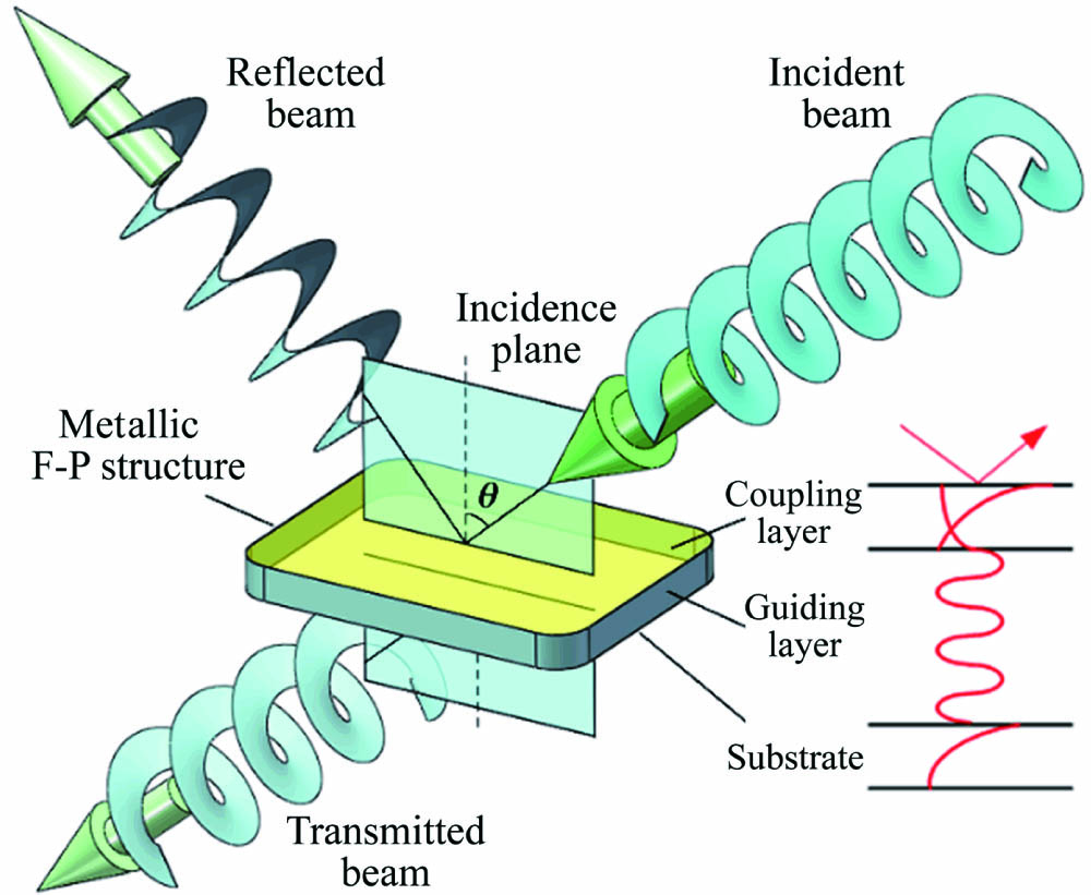
    The schematic in Fig. 1 shows an incident VB reflected by an SMCW chip, and the insert shows the distribution of a specific UOM. The SMCW structure is similar to the metal–dielectric–metal (MDM) scheme that is widely studied in plasmonics. Instead of the basic symmetric and antisymmetric modes, our interest mainly focuses on the oscillating modes of high order. In our experiment, a 0.23 mm thick glass slab with excellent optical parallelism is sandwiched between two silver films. The excited UOMs will propagate along the millimeter thick glass layer until all of the energy is leaked out through the metal claddings. The upper coupling layer is made of 30 nm thick silver film, which facilitates the direct coupling into the chip from free space. No high index prism or coupling grating is needed, since the effective index of UOMs can approach zero. The metal substrate is also 30 nm thick, so both reflection and transmission can be detected. Theoretically, it is simple to calculate the reflectivity and field distribution of a Gaussian beam via the transfer matrix method. What we are more interested in is the reflection of an incident beam carrying OAM at the resonance of the UOMs.

    Refraction of an optical VB by an SMCW chip and the E-field distribution of an oscillating UOM at resonance (red line).

    Figure 1.Refraction of an optical VB by an SMCW chip and the E-field distribution of an oscillating UOM at resonance (red line).

    A VB generated by a spiral phase plate is incident on the surface of the SMCW with an angle θ, where the topological charge is l=1, and the wavelength and the beam waist are 532 nm and 0.5 mm, respectively. The SMCW chip is placed on a goniometer to carry out angular scanning. The reflection spectrum is recorded by a photoelectric detector, and the reflected pattern is detected by a charge-coupled device (CCD). The typical reflected patterns measured around a UOM’s resonance are illustrated in Fig. 2, whilst the corresponding reflectivity is shown in Fig. 3. Note that the angle corresponding to Fig. 2(c) is located close to the center of a resonant dip, and the reflected spots are significantly distorted in comparison with the incident beam. Careful examination shows that several outer rings other than the inner ring exist in the reflected spot, which evolve continuously as we scan the incident angle gradually. A twisted M-line appears from one side, moves across the light spot, and disappears on the other side. As the twisted dark line passes through the beam center, the reflectivity decreases to a minimum, leading to the resonant dip.

    (a) Optical field of the incident beam generated by a spiral phase plate with l = 1. (b), (c), and (d) Optical field of the reflected beam at 9.42, 9.50, and 9.52 deg, respectively. The intensity is normalized to the maximum of the incident light spot.

    Figure 2.(a) Optical field of the incident beam generated by a spiral phase plate with l = 1. (b), (c), and (d) Optical field of the reflected beam at 9.42, 9.50, and 9.52 deg, respectively. The intensity is normalized to the maximum of the incident light spot.

    (Top) Experimentally measured reflectivity of a VB reflected by the SMCW chip; (bottom) numerically simulated reflectivity of a planar wave model via the transfer matrix method. The permittivity of silver is based on the Drude model εAg = −13.9235 + 0.7233i, and the permittivity of the guiding layer is 2.25.

    Figure 3.(Top) Experimentally measured reflectivity of a VB reflected by the SMCW chip; (bottom) numerically simulated reflectivity of a planar wave model via the transfer matrix method. The permittivity of silver is based on the Drude model εAg = −13.9235 + 0.7233i, and the permittivity of the guiding layer is 2.25.

    The inner ring is formed by the direct reflection of incidence at the chip surface. The physics behind the occurrence of outer rings can be attributed to the random scattering caused by the natural roughness of the silver film, which enables the coupling between different UOMs of different orders in all azimuthal directions[15]. Thus, hollow light cones other than the reflected spot are formed due to the leakage of the UOMs. The outer rings in Figs. 2(c) and 2(d) are brighter than that in Fig. 2(b), while the inner ring shows an opposite manner. The reason can be explained as follows: critical coupling of the UOMs can be achieved when destructive interference between the leakage of the UOMs and the direct reflection at the upper surface is complete, and thus the inner ring at resonance is dim. On the other hand, most energy is shifted to UOMs at resonance, so the mode leakage is enhanced to produce brighter outer rings. Given the origins of the inner and outer rings, the rest of this paper will focus on the physics behind the twisted M-line.

    In Fig. 3, the measured reflectivity of a VB is compared with the simulated results. Since the number of the UOMs in the sub-millimeter thick SMCW is very large, we only show a part of the spectrum for clarity. The FWHM of the dips in the experiment is much wider, which can be attributed to the different incidence conditions and will be explained later. In Fig. 4, we show the reflection of an ordinary Gaussian beam near resonance, which differs significantly from the VB case. Figures 4(b) to 4(d) show that the Gaussian beam is stretched at first, then a curved M-line appears corresponding to the resonant angle, and finally the Goos–Hänchen effect manifests itself as a discernible shift of the beam peak.

    Evolution of the M-line in a reflected Gaussian beam under the same experimental conditions. The coupling angle of the resonant dip is around 9.13 deg. The intensity is normalized to the maximum of the reflected light spot in (b).

    Figure 4.Evolution of the M-line in a reflected Gaussian beam under the same experimental conditions. The coupling angle of the resonant dip is around 9.13 deg. The intensity is normalized to the maximum of the reflected light spot in (b).

    3. Theoretical Model

    First, we demonstrate the high angular sensitivity of the UOMs, which is crucial to sensing the phase pattern of a VB. To clarify the inner relation among the UOMs, the surface plasmon (SP) mode, the symmetric (TM0) mode, and the anti-symmetric (TM1) mode, the reflection spectra of a prism-coupled SMCW chip are plotted in Fig. 5. Note that the prism is not necessary for the coupling of the UOMs, since they can be excited at a small incidence angle. The prism facilitates the coupling of the SP and the symmetric modes since they can only be excited under the attenuated total reflection (ATR) condition. As the thickness of the guiding layer increases, the TM0 and TM1 modes degenerate into the SP mode, while the remaining TE and TM modes degenerate into the UOMs. For an SMCW chip of millimeter scale, the total number of the UOMs is in the order of 103, and the corresponding FWHM of each resonance dip is much narrower than that of the SP resonance. Consequently, higher angular resolution can be obtained via the UOMs.

    Reflection spectra of a prism-coupled SMCW chip as a function of film thickness and incident angle. θc is the critical angle for total reflection of the guiding layer.

    Figure 5.Reflection spectra of a prism-coupled SMCW chip as a function of film thickness and incident angle. θc is the critical angle for total reflection of the guiding layer.

    Let us further consider the finesse F of the chip, which is defined by the ratio of the mode spacing Δθ to the mode width wθ. From the dispersion relation of UOMs, it is easy to find that the mode spacing can be approximated as Δθ1/sin2θ, and the mode width is wθ=2[Im(βrad)]kngcosθ,where k is the free space wavenumber, ng is the refractive index of the guiding layer, and the radiative damping is[16]Im(βrad)exp(2iαs)dsinθ.s, d are the thickness of the coupling and guiding layers, respectively, and α is the attenuation coefficient of the metal cladding. Substituting Eqs. (1) and (2), the finesse of the UOMs can be written as Fngkdexp(2iαs).

    Under weak coupling condition, there is exp(2iαs)1. For the millimeter thick waveguide, there is kd103. Thus, the finesse of the proposed SMCW chip is very high, whilst a typical Fabry–Perot cavity only has finesse in the order of 102. Using the same parameters as we have applied for the numerical simulation in Fig. 3, the finesse can be evaluated as 3.804×10³. The high finesse of our resonant chip can also be illustrated by the extremely narrow dips in the numerical simulation based on planar incidence in Fig. 3. Consequently, the UOMs can provide high angular resolution to facilitate the phase structure sensing of a VB.

    Next, we consider a Laguerre–Gaussian beam carrying an optical vortex with a topological charge l, whose phase Φ is given by[17]Φ=kρ2z2(z2+zR2)+lφ+kz(2p+|l|+1)arctan(z/zR).

    For the parameters, zR=kw02/2 is the Rayleigh range, w0 is the beam waist, and p is the radial index. The last term in Eq. (4) is the Gouy phase. Let us assume that the Poynting vector S is always perpendicular to the helicoidal phase plane, which follows SΦρeρ+Φρφeφ+Φzez.

    Inserting Eq. (4) into Eq. (5) and neglecting the Gouy phase, we have S/kρzz2+zR2eρ+lkρeφ+ez.

    As shown in Fig. 6(a), it is simple to plot the distribution of S on different cross sections of the beam as the light propagates. Obviously, the conventional incident angle θ defined by the beam axis cannot represent the actual incident angle at specific positions. Thus, when a VB is refracted by an SMCW chip with high angular sensitivity, great care is required.

    (a) Phase structure and related energy flux S⇀ distribution (black arrow) in the beam cross sections at different propagation distances. (b) The distribution of the energy flux vector (red arrow) at a tilted cross section (blue circle) due to a nonzero incident angle θ.

    Figure 6.(a) Phase structure and related energy flux S distribution (black arrow) in the beam cross sections at different propagation distances. (b) The distribution of the energy flux vector (red arrow) at a tilted cross section (blue circle) due to a nonzero incident angle θ.

    When the beam is incident with a nonzero θ, the cross section of incidence is also tilted by θ. An example is shown in Fig. 6(b), where a VB travels along the z axis, and the vector n denotes the normal to the chip surface of the SMCW. Apparently, the local incident angle θL at a specific point should be defined as the angle between the normal n and the energy flux vector S for each point.

    For the calculation of the local incident angle θL in the Cartesian coordinates, Eq. (6) can be recast into SSxex+Syey+Szez, with Sx/Sz=ρzz2+zR2cosφlkρsinφ,Sy/Sz=ρzz2+zR2sinφ+lkρcosφ.

    In view of Fig. 6(b), the normal to the chip surface n can be defined as (sinθ,0,cosθ). Finally, we can write down the local incident angle θL as θL=arccoscosθSzsinθSxSx2+Sy2+Sz2.

    Eq. (8) can be applied to calculate the distribution of θL over the titled cross section at different propagation distances z. Note that the VB has a spread at the local incident angle θL, which explains the wide FWHM observed for VB incidence, as shown in Fig. 3.

    4. Results and Discussion

    As mentioned in Section 2, the outer rings in Fig. 2 are formed by random scattering of the natural roughness and the coupling between UOMs. The inner ring is formed mainly due to the direct reflection of the VB. Based on the proposed theory, the patterns of the inner ring can be simulated by taking the local incident angle θL into account, and the results are shown in Fig. 7.

    Simulated inner ring and the M-line of the reflected VB (l = 1) near a resonance, where the parameters are the same as those used in Fig. 3. The beam waist is 0.5 mm, and the propagation distance is z = 50 cm.

    Figure 7.Simulated inner ring and the M-line of the reflected VB (l = 1) near a resonance, where the parameters are the same as those used in Fig. 3. The beam waist is 0.5 mm, and the propagation distance is z = 50 cm.

    The similarity between Figs. 2 and 7 is obvious, so the proposed model fits well with the experiments. Figure 7 shows the whole process of how the reflected beam is distorted by a twisted M-line. The M-line emerges from the central phase singularities, moves across the beam, and finally disappears into the singularity again. Since the M-line varies continuously as a function of the incident angle, the M-line method via UOMs provides sufficient sensitivity for the phase structure detection of the light beam carrying OAM.

    For large incident angle θ, the density of the UOMs increases, which enables the possibility to excite several UOMs simultaneously via a single beam. Thus, more information can be obtained when more complicated phase structures are detected. An example is shown in Fig. 8, where VBs of different charges are incident with a large angle θ=30deg. For both cases of l=1 and l=2, the twisted M-lines in the intensity profiles match well with the phase patterns. Furthermore, since the large topological charge corresponds to large phase variation, two UOMs (mode a and mode b) are successfully excited in the case of l=2, resulting in two twisted M-lines across the beam. In comparison, the number of M-lines in the case of l=1 is only one. Note that we should not read too much into the center region of the beam, where the phase is ill defined at the singularity.

    (a), (d) Intensities and (b), (e) phase structures of the reflected beams with different topological charge l; (c), (f) the phase structures of the incident beams are also plotted for comparison. The incident angle is θ = 30 deg, and the rest parameters are the same as those used in Fig. 7.

    Figure 8.(a), (d) Intensities and (b), (e) phase structures of the reflected beams with different topological charge l; (c), (f) the phase structures of the incident beams are also plotted for comparison. The incident angle is θ = 30 deg, and the rest parameters are the same as those used in Fig. 7.

    5. Conclusion

    In conclusion, we investigate the reflection of a VB by an SMCW chip. Owing to the high angular resolution of the UOMs, the phase structure of the reflected beam is well described by the evolution of twisted M-lines. A very simple model is proposed based on defining the local incident angle, and the theoretical prediction matches well with the experiments. This work provides an effective approach to the imaging and sensing of complicated phase structures.

    References

    [1] L. Allen, M. W. Beijersbergen, R. J. C. Spreeuw, J. P. Woerdman. Orbital angular momentum of light and the transformation of Laguerre–Gaussian laser modes. Phys. Rev. A, 45, 8185(1992).

    [2] K. Y. Bliokh, F. J. Rodríguez-Fortuño, F. Nori, A. V. Zayats. Spin-orbit interactions of light. Nat. Photon., 9, 796(2015).

    [3] M. Chen, M. Mazilu, Y. Arita, E. M. Wright, K. Dholakia. Dynamics of microparticles trapped in a perfect vortex beam. Opt. Lett., 38, 4919(2013).

    [4] G. Xie, L. Li, Y. Ren, H. Huang, Y. Yan, N. Ahmed, Z. Zhao, M. P. J. Lavery, N. Ashrafi, S. Ashrafi, R. Bock, M. Tur, A. F. Molisch, A. E. Willner. Performance metrics and design considerations for a free-space optical orbital-angular-momentum–multiplexed communication link. Optica, 2, 357(2015).

    [5] W. Qi, R. Liu, L. Kong, Z. Wang, S. Huang, C. Tu, Y. Li, H. Wang. Double-slit interference of single twisted photons. Chin. Opt. Lett., 18, 102601(2020).

    [6] Y. Li, Y. Liu, X. Ling, X. Yi, X. Zhou, Y. Ke, H. Luo, S. Wen, D. Fan. Observation of photonic spin Hall effect with phase singularity at dielectric metasurfaces. Opt. Express, 23, 1767(2015).

    [7] S. Zheng, J. Wang. On-chip orbital angular momentum modes generator and (de)multiplexer based on trench silicon waveguides. Opt. Express, 25, 18492(2017).

    [8] P. F. Chimento, P. F. A. Alkemade, G. W. Hooft, E. R. Eliel. Optical angular momentum conversion in a nanoslit. Opt. Lett., 37, 4946(2012).

    [9] Y. Yang, L. Wu, Y. Liu, D. Xie, Z. Jin, J. Li, G. Hu, C. Qiu. Deuterogenic plasmonic vortices. Nano. Lett., 20, 6774(2020).

    [10] P. K. Tien, R. Ulrich, R. J. Martin. Modes of propagating light waves in thin deposited semiconductor films. Appl. Phys. Lett., 14, 291(1969).

    [11] G. Chen, Z. Cao, J. Gu, Q. Shen. Oscillating wave sensors based on ultrahigh-order modes in symmetric metal-clad optical waveguides. Appl. Phys. Lett., 89, 081120(2006).

    [12] J. Gu, G. Chen, Z. Cao, Q. Shen. An intensity measurement refractometer based on a symmetric metal-clad waveguide structure. J. Phys. D, 41, 2824(2008).

    [13] H. Dai, L. Yuan, C. Yin, Z. Cao, X. Chen. Direct visualizing the spin Hall effect of light via ultrahigh-order modes. Phys. Rev. Lett., 124, 053902(2020).

    [14] X. Zhou, L. Sheng, X. Ling. Photonic spin Hall effect enabled refractive index sensor using weak measurements. Sci. Rep., 8, 1221(2018).

    [15] H. Dai, B. Jiang, C. Yin, Z. Cao, X. Chen. Ultralow-threshold continuous-wave lasing assisted by a metallic optofluidic cavity exploiting continuous pump. Opt. Lett., 43, 847(2018).

    [16] X. Liu, Z. Cao, P. Zhu, Q. Shen, X. Liu. Large positive and negative lateral optical beam shift in prism-waveguide coupling system. Phys. Rev. E, 73, 056617(2006).

    [17] L. Allen, M. Beijersbergen, R. Spreeuw, J. Woerdman. Orbital angular momentum of light and transformation of Laguerre Gaussian laser modes. Phys. Rev. A, 45, 8185(1992).

    Cheng Yin, Xuefen Kan, Kun Guo, Tao Wang, Jiangming Xu, Qingbang Han, Jian Wu, Zhuangqi Cao. Highly twisted M-line of a vortex beam due to the coupling of ultrahigh-order modes[J]. Chinese Optics Letters, 2021, 19(7): 071403
    Download Citation