
Xin Chen, Jinsong Gao, Bonan Kang. Experimental realization of a switchable filter based on a dynamically transformable array[J]. Chinese Optics Letters, 2018, 16(8): 081202
- Chinese Optics Letters
- Vol. 16, Issue 8, 081202 (2018)
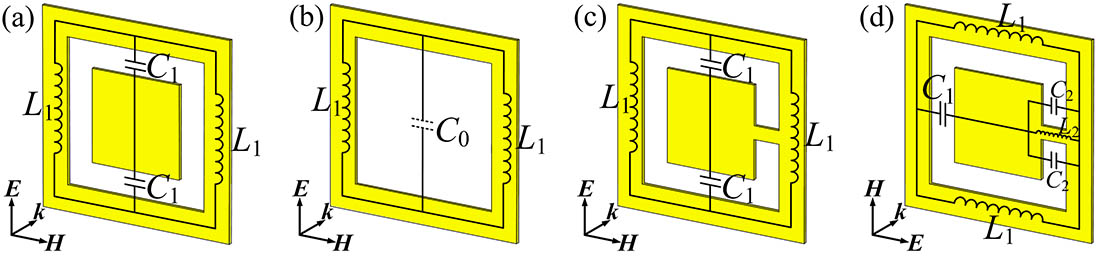
Fig. 1. Equivalent circuit model for the TE polarization of (a) a square loop aperture element, (b) a square aperture element, (c) a shorted square loop aperture element; and for TM polarization of (d) a shorted square loop aperture element.
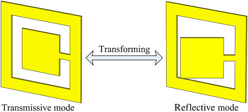
Fig. 2. Operational principle of the model: morphology transforming between two different elements.
Fig. 3. (a) 3D schematic of the unit cell, where T x = T y = 15 mm a = 6 mm b = 5.5 mm c = d = 0.5 mm z direction. (b) The frequency response obtained from full-wave simulation with different values of θ
Fig. 4. Morphologies of the sample with external stimulation of (a) high temperature and (b) low temperature.
Fig. 5. Measurement results of the sample at different temperatures under (a) TE polarization and (b) TM polarization.
Fig. 6. Measurement results of the sample at different temperatures under (a) TE polarization and (b) TM polarization for different cycles.
Fig. 7. Distributions of (a), (c) the surface currents and (b), (d) the electric fields for TE polarization under normal incidence when (a), (b) θ = 180 ° θ = 130 °
Fig. 8. Distributions of (a), (c) the surface currents and (b), (d) the electric fields for TM polarization under normal incidence when (a), (b) θ = 180 ° θ = 130 °

Set citation alerts for the article
Please enter your email address
© Copyright 2018-2021 | Chinese Laser Press. All Rights Reserved 沪ICP备15018463号-20