1State Key Laboratory of Integrated Optoelectronics, College of Electronic Science and Engineering, Jilin University, Changchun 130012, China
2Key Laboratory of Optical System Advanced Manufacturing Technology, Changchun Institute of Optics, Fine Mechanics and Physics, Chinese Academy of Sciences, Changchun 130033, China
Xin Chen, Jinsong Gao, Bonan Kang, "Experimental realization of a switchable filter based on a dynamically transformable array," Chin. Opt. Lett. 16, 081202 (2018)
Copy Citation Text
We introduce a geometrically reconfigurable metasurface whose artificial “atoms” will reorient within unit cells in response to a thermal stimulus in the microwave spectrum. It can alternate between two contrasting behaviors under different temperatures and serve as a switchable filter that allows the incident energy to be selectively transmitted or reflected with an excess of 10 dB isolation at certain frequencies for both polarizations. The experimental results are consistent with the theoretical simulations, verifying the availability of an innovative method for manipulating electromagnetic waves with the merits of higher controllability for dynamic behavior and greater flexibility in the design process.
Metamaterials are artificial electromagnetic media that could exhibit several exotic phenomena that cannot be normally found in nature[1–4]. A kind of single layer metamaterial that consists of a flat periodic or quasi-periodic array, called a metasurface, could create many possibilities for manipulating the propagation behavior of electromagnetic waves while maintaining an ultrathin thickness that is smaller than the wavelength of interest[5–11]. Compared with a passive metasurface whose frequency response is fixed once the fabrication is finished, the electromagnetic performance of a reconfigurable metasurface can be modulated with time by integrating dynamic components into the design. Some reconfigurable metasurfaces with the functionalities of tuning, switching, or sensing have drawn enormous attention in recent years. One well-known method is to introduce the active elements into the structure of the metasurface, such as a semiconductor[12–14], ferrite[15], or liquid crystal[16,17]. However, these measures always exhibit unavoidable drawbacks including insertion losses, passband fluctuations, complexity of fabrication, and lack of design flexibility. Alternatively, the properties of metasurfaces can be directly modified by reconfiguring the fundamental building blocks of the structure[18–21]. But there are also some defects in previous works involving high operating temperature, poor reversibility, or small modulation range, so achieving a high efficient reconfigurable metasurface with an arbitrary control of technology and convenience in practical applications remain key issues in the field of electromagnetic waves.
In this present work, we provide a feasible method to realize a switchable metasurface with superior performance and convenience in practical applications. We design and fabricate a geometrically reconfigurable array using shape memory alloys (SMAs), which suffer from a high temperature sensitivity that can cause changes to the geometry of the unit cells with the proper variation in temperature. Utilizing the reversible conversion between the two kinds of arrays through thermoregulating, an all-metal metasurface could realize the working mode of transmission or reflection at the frequencies of interest, as we expect, with a good isolation. We use equivalent circuit models to predict the electromagnetic behavior of the surface, and the switching function is demonstrated by full-wave analysis. The measured results coincide with the simulations, making the dynamically transformable array a practicable method for greatly improving the flexibility and simplicity in the design process of a reconfigurable metasurface in different electromagnetic spectra with alternative resonant structures.
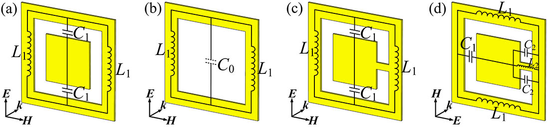
When the configuration of the unit cell is a square loop aperture element, as shown in Fig. 1(a), the long bars in the vertical direction lead to the inductance across an equivalent transmission line for TE polarization and the horizontal gaps act like capacitance primarily in parallel with , the parallel LC resonator becomes a classic passband filter with a transmission peak in the spectrum of interest. If we take away the patch in the middle of the element, as shown in Fig. 1(b), the unit cell becomes a square aperture element where the wider gaps bring about a smaller capacitance that cannot produce a valid resonance with the high quality factor of the parallel circuit. The transmission characteristics of the two elements will not change for TM polarization due to the symmetry of the structures. When the patch connects to the right edge of the aperture with a cantilever, the equivalent circuit model can be thought of as two different transmission line circuits corresponding to TE and TM polarization, respectively, as shown in Figs. 1(c) and 1(d). For TE polarization the equivalent circuit model is the same as in Fig. 1(a), but for TM polarization the cantilever converts the region of existing capacitance to the approximate inductance , and capacitors remain out of the connection with a smaller capacitance . The two parallel LC resonators generate two resonant peaks in the transmission spectrum, contrary to the case of TE polarization; the lower resonant frequency is mostly determined by and , which have the larger values, whereas the higher resonant frequency mainly depends on the smaller inductance and the capacitance . Because of the huge differences between and , and and , the two resonant frequencies are separated by a large distance in the transmission spectrum, so we have to consider the onset of grating lobes for TM polarization. The frequency where a grating lobe is encountered under normal incidence is determined by[22]the grating lobe indices (, ) that satisfy Eq. (1) are those values different from (0, 0), and and denote the element spacing in the x direction and y direction, respectively.
Sign up for Chinese Optics Letters TOC. Get the latest issue of Chinese Optics Letters delivered right to you!Sign up now
Figure 1.Equivalent circuit model for the TE polarization of (a) a square loop aperture element, (b) a square aperture element, (c) a shorted square loop aperture element; and for TM polarization of (d) a shorted square loop aperture element.
Qualitative analysis from equivalent circuit models implies that we could modify the transmission characteristics of the surface by moving the patch and then switching the morphology of the unit cell between two different geometrical shapes corresponding to the transmissive mode and the reflective mode, respectively, at a certain frequency. One possible method is connecting the patch and the bar with a cantilever that could bend out of the aperture, as shown in Fig. 2. If the patch is bent out of the surface for TE polarization, the morphology of the unit cell will convert from the transmissive structure of the resonant element to the reflective structure of the approximately inductive element, which leads to a great change in the transmission characteristics of the surface; when switching in the same way for TM polarization, it will have a huge influence on the lower resonant frequency because the large distance brings about a small capacitance parallel with the horizontal bars, as previously mentioned; meanwhile, the values of and will also change due to the variation of the spatial relationship between the patch and the vertical bar on the right side, which results in the drift of the higher resonant frequency. The above indicates the operational principle of the workable model.
Figure 2.Operational principle of the model: morphology transforming between two different elements.
For getting a vivid illustration of the behavior of the equivalent circuit models, full-wave analysis of the metasurface is performed by using Computer Simulation Technology (CST) software. The transmission spectrum of the filter is determined by solving Maxwell’s equations with the finite integration technique; the numbers of cells per wavelength and cells per max model box edge are both 15 for the whole model structure. A three-dimensional (3D) view of the unit cell structure is shown in Fig. 3(a) including the design parameters. Figure 3(b) shows that the transmission characteristics of the metasurface highly depend on the morphology of the unit cell under normal incidence for both polarizations, demonstrating the consequences predicted by equivalent circuit models. When the cantilever stays in the aperture of the surface and for TE polarization, the unit cell becomes a resonant structure composed of the shortest square loop aperture element that could transmit the energy impinging on it at 14.3 GHz and exhibit a small transmission loss of less than 0.25 dB. When the cantilever bends out of the aperture and , we obtain an embossed reflector with a good isolation of more than 10.5 dB from the transmissive mode at the original resonant frequency, certifying the signal rejection in the mentioned frequency band. For TM polarization we verify that the surface has the ability of switching at 6.8 GHz but suffers a failure at 20 GHz, where we see the grating lobe as predicted by Eq. (1) no matter what the value of is. Thus, not taking account of the invalid dual-band switchable filter, we develop a freestanding switchable bandpass filter using a thin self-supporting and air-spaced metasurface composed of a transmutable array in which the transmittance can be switched at 14.3 GHz for TE polarization and at 6.8 GHz for TM polarization.
Figure 3.(a) 3D schematic of the unit cell, where , , , and ; the plane wave propagates along the z direction. (b) The frequency response obtained from full-wave simulation with different values of for both polarizations.
In order to change the shape of the original unit cell properly, one simple and effective method is that we machine the sample using SMA that have been characterized by the changes in its transformation temperatures and its two-way shape memory effect. It can recover a shape not only on heating but also during cooling[23]; in this way, a sample takes two different shapes depending on the temperature.
The experimental alloy is prepared by induction melting of high-purity initial elements with a nominal composition of copper (69.61wt.%), zinc (25.7wt.%), aluminum (3.81wt.%), nickel (0.8wt.%), lanthanum (0.04wt.%), and cerium (0.04wt.%) under an argon atmosphere at 1250°C and homogenized at 850°C for 24 h. The percentage value is the mass fraction of every component element. After furnace cooling the ingot is hot-rolled and cold-rolled into a plate with a thickness of 0.5 mm, then a sample of in dimension is spark cut from the plate and the aforementioned element is realized by a machining operation, the surface is electropolished until all cutting marks are completely removed[24–26].
By using the method mentioned in Ref. [27], we get the values of the characteristic temperatures: , , , and , where , , , and represent the martensitic transformation start and finish temperatures and the austenite transformation start and finish temperatures, respectively, and the temperature hysteresis .
The process of thermal cycling under an applied stress to induce the two-way shape memory effect is commonly referred to as two-way training. First, heat the surface higher than 70°C to the high temperature phase with electric heaters, then bend the patch of each unit cell out of the aperture slowly to the deformation position where the value of is about 120°; second, sustain the morphology with stress by cooling it to room temperature; third, unload the stress and the cantilever will spring back slightly; and last, reheat the surface to the high temperature phase and the cantilever continues to move spontaneously in the same direction until the value of is about 170° for shape recovery.
By repeating the above cycle for 6 times, the surface possesses the ability of switching its morphology, alternating between two different shapes, without an external force, on heating and cooling: when the sample is heated over 58°C, the appearance of the unit cell begins switching to the transmissive morphology by depressing the cantilever downward until the temperature is higher than 70°C and then the value of is about 170,° as shown in Fig. 4(a); the whole process takes less than 5 s and the response time highly depends on the distance between the electric heaters and the sample. After the temperature of the sample drops below 64°C, the patch raises upward to recover the reflective morphology, and finally the value of is about 130° at room temperature, as shown in Fig. 4(b).
Figure 4.Morphologies of the sample with external stimulation of (a) high temperature and (b) low temperature.
For characterizing the behavior of the sample, an experiment is carried out in a microwave anechoic chamber; two electric heaters are used for heating the sample to assure that the temperature is high enough. When heating the sample to the high temperature phase for TE polarization, we find that the passband is centered at 15 GHz with a small insertion loss of 0.4 dB, as shown in Fig. 5(a); if we stop heating and the temperature of the sample drops down low enough, more than 10 dB attenuation will be observed at the original resonance frequency. For TM polarization the peak value is at 8.2 GHz and we get an even better isolation of 14 dB between the two working modes, as shown in Fig. 5(b). The curve trends of measurements and simulations are similar to each other for the same value of . The slight frequency deviations and expansion of the passband range may be ascribed to the manufacturing tolerance and the disparity of the bending angle produced in the training process. In addition, infinite arrays are simulated while the finite surface is measured. However, this experiment can be used to confirm the accuracy of our prediction in the previous sections. We also show the measurement results of the sample after several temperature cycles in Fig. 6. To survey the durability of the metal surface, we can see that the performance will not display the noticeable degradation until the number of cycle exceeds 10.
Figure 5.Measurement results of the sample at different temperatures under (a) TE polarization and (b) TM polarization.
To better understand the physical picture for the variation of the transmission characteristics, we can gain some insight into the changes of the electric field strength and the surface current distribution on the surface at the resonance frequency, as shown in Figs. 7 and 8 when the value of is different for both polarizations. We add the arrows to represent the directions of the surface current more clearly during the half cycle.
Figure 7.Distributions of (a), (c) the surface currents and (b), (d) the electric fields for TE polarization under normal incidence when (a), (b) and (c), (d) at 14.3 GHz.
Figure 8.Distributions of (a), (c) the surface currents and (b), (d) the electric fields for TM polarization under normal incidence when (a), (b) and (c), (d) at 6.8 GHz.
For TE polarization, the maximal surface current is induced around the two flanks of the aperture and flows along the edges of the inner patch and outer bars in the opposite directions at 14.3 GHz, as shown in Fig. 7(a), which results in the conspicuous charge accumulation in the capacitors derived from the gaps at the top and bottom when the value of is 180°. Thus, the strongest electric fields are distributed on the edges of the gaps, as shown in Fig. 7(b), corresponding to the maximal transmittance in the spectrum of consideration. The difference is that the surface current declines significantly along the flow direction when the patch bends out of the aperture at the same frequency, as shown in Fig. 7(c). The reduction of the surface current weakens the charge accumulation and thus the electric field strength, as displayed in Fig. 7(d). Another profound consequence is that the variation of the surface current distribution on the surface destroys the original resonance, leading to an obvious descent of the transmittance at the initial resonant frequency when the value of is 130°. This means that the peak of the transmission spectrum is corresponding to the emergence of the maximal surface current on the surface, hence we can manipulate the transmission characteristics of the metasurface by transforming the morphology of the unit cell and then altering the surface current distribution on the metal structure.
The change rules of the electric field strength and surface current distribution on the surface for TM polarization at 6.8 GHz are like that for TE polarization when the value of is different, as shown in Fig. 8. From the above descriptions we get a deeper understanding of the switching mechanism of the metasurface.
In this article, we propose a geometrically reconfigurable metasurface as a flexible platform for realizing a switchable spatial filter with the features of good reversibility and high switch isolation in the microwave part of the spectrum. This is accomplished by fabricating a transformable array whose unit cells could convert their structure from one geometrical shape to the other spontaneously and repeatedly in response to a thermal stimulation. Both simulations and measurements have been carried out to validate its performance, demonstrating that a switchable attenuation of more than 10 dB will occur at disparate frequencies for different polarizations during the cycle of heating and cooling. A further physical mechanism is shown by contrasting the distributions of the electric field and surface current on the surface at the same frequency for the two working modes. With the advantages of more flexibility for the design procedure and higher controllability for the dynamic behavior, the design methodology in this paper can be applied to other diverse functions such as high-sensitivity sensing, tunable filtering, frequency-selective detection, and multispectral imaging.
Xin Chen, Jinsong Gao, Bonan Kang, "Experimental realization of a switchable filter based on a dynamically transformable array," Chin. Opt. Lett. 16, 081202 (2018)