
Liangchao Fan, Zhi Huang, Quanjiang Lü, Guiwu Liu, Guanjun Qiao, Junlin Liu. Effect of Two-Step Annealing on Optoelectronic Properties of Lead Sulfide Thin Films[J]. Acta Optica Sinica, 2023, 43(10): 1031001
- Acta Optica Sinica
- Vol. 43, Issue 10, 1031001 (2023)
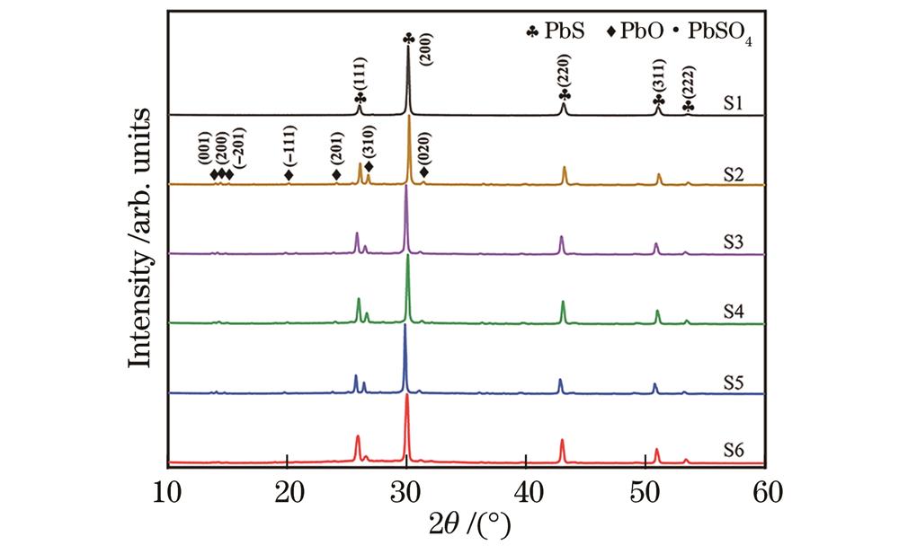
Fig. 1. XRD patterns of samples S1-S6

Fig. 2. Optical microscope surface morphologies of samples S1-S6. (a) Sample S1; (b) sample S2; (c) sample S3; (d) sample S4; (e) sample S5; (f) sample S6
Fig. 3. SEM surface morphologies of samples S1-S6. (a) Sample S1; (b) sample S2; (c) sample S3; (d) sample S4; (e) sample S5; (f) sample S6
Fig. 4. Schematic diagram of optoelectronic property test and optoelectronic properties of PbS thin films at different optical power densities. (a) Schematic diagram of optoelectronic property test; (b) Iph; (c) R; (d) D*
Fig. 5. Thicknesses and optoelectronic properties of PbS thin films. (a) Thicknesses of samples S1-S6; (b) Idark of samples S2-S6;(c) R of samples S2-S6; (d) D* of samples S2-S6
Fig. 6. Response diagram of sample S5 at high frequency. (a) Normalized response curve at 4 kHz; (b) partial magnification of Fig. 6(a)

Set citation alerts for the article
Please enter your email address
© Copyright 2018-2021 | Chinese Laser Press. All Rights Reserved 沪ICP备15018463号-20