
Jiayang Wu, Pan Cao, Ting Pan, Yuxing Yang, Ciyuan Qiu, Christine Tremblay, and Yikai Su. Compact on-chip 1×2 wavelength selective switch based on silicon microring resonator with nested pairs of subrings[J]. Photonics Research, 2015, 3(1): 9
- Photonics Research
- Vol. 3, Issue 1, 9 (2015)
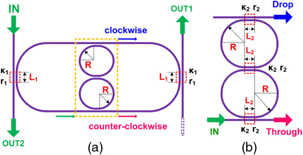
Fig. 1. (a) Schematic configuration of the proposed MRR with one NPS. (b) Zoom-in view of NPS marked with dashed box in (a).
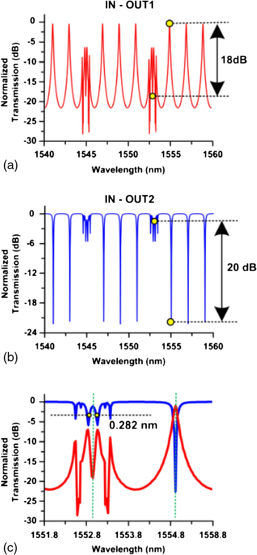
Fig. 2. (a) Normalized transmission spectrum from IN to OUT1. (b) Normalized transmission spectrum from IN to OUT2. (c) Zoom-in view of (a) and (b) in the wavelength range of 1551.8–1555.8 nm.
Fig. 3. Micrograph of the fabricated devices with (a) one and (b) two NPSs.
Fig. 4. (a) Measured transmission spectrum from IN to OUT2 of the fabricated device with one NPS. (b) Zoom-in spectrum around one split resonance at λ 1 1 ) and (2 ). (c)–(f) Measured transmission spectra from IN to OUT1 when the power applied to the microheater is 0.0, 5.8, 11.1, and 16.1 mW, respectively.
Fig. 5. Measured transmission spectra from IN to OUT1 of the fabricated device with two NPSs when the power applied to the microheater along one of the two NPSs is (a) 0.0, (b) 4.5, (c) 8.8, (d) 13.0, (e) 17.0, and (f) 20.7 mW, respectively.
Fig. 6. Experimental setup for system demonstration of dynamic channel routing using the fabricated device. VOA, variable optical attenuator.
Fig. 7. Eye diagrams of 10 Gb / s λ 1 – λ 4 10 Gb / s λ 1 ′ – λ 6 ′
Fig. 8. BER curves measured with the fabricated devices with (a) one and (b) two NPSs.

Set citation alerts for the article
Please enter your email address
© Copyright 2018-2021 | Chinese Laser Press. All Rights Reserved 沪ICP备15018463号-20