Abstract
We propose and experimentally demonstrate compact on-chip 1 × 2 wavelength selective switches (WSSs) based on silicon microring resonators (MRRs) with nested pairs of subrings (NPSs). Owing to the resonance splitting induced by the inner NPSs, the proposed devices are capable of performing selective channel routing at certain resonance wavelengths of the outer MRRs. System demonstration of dynamic channel routing using fabricated devices with one and two NPSs is carried out for 10 Gb∕s non-return-to-zero signal. The experimental results verify the effectiveness of the fabricated devices as compact on-chip WSSs.1. INTRODUCTION
Ever-increasing network capacity and efficiency are driving the demand for high-performance channel management technologies in wavelength division multiplexing (WDM) optical communication networks. Reconfigurable optical add–drop multiplexers (ROADMs), which enable flexible management and reconfigurable provisioning of wavelength channels, are key building blocks for next-generation WDM networks [1,2]. Wavelength selective switches (WSSs) are core components in ROADMs [1–5]. By controlling the transmission of each individual channel, a WSS serves as a reconfigurable node to interchange wavelength channels amongst various routes.
A number of schemes have been proposed to implement WSSs based on microelectromechanical systems (MEMS) [6,7], liquid crystal (LC) [8,9], silica-based planar lightwave circuits (PLCs) [10,11], and silicon photonic wire waveguides (PWWs) [12–14]. Among them, WSSs based on silicon PWWs can offer a competitive edge in the deployment of cost-effective on-chip ROADM systems due to the capability for large-scale integration leveraging from well-developed silicon-based fabrication technologies. Moreover, the high refractive-index contrast and strong light confinement of silicon PWWs fabricated on a silicon-on-insulator (SOI) platform also allow for photonic devices with reduced sizes. Since silicon microring resonators (MRRs) are compact comb filters employed for optical networks-on-chip (NoCs) [15,16], it would be desired to implement an integrated WSS by selectively routing certain resonance channels of a MRR. However, it has been proved to be difficult to control certain resonances of a single MRR without affecting the others [17].
In this paper, a scheme to implement compact on-chip WSSs based on silicon MRRs with nested pairs of subrings (NPSs) is proposed and experimentally demonstrated. Due to the resonance splitting caused by the inner NPSs, the proposed devices can be used to selectively route certain resonance channels of the outer MRRs without affecting the unrouted channels. Compared to on-chip silicon WSSs implemented by Mach–Zehnder interferometers (MZIs) [13] or cascaded MRRs [14], the proposed devices based on embedded ring resonators [18–21] possess more compact footprints due to an effective utilization of the area inside the resonant cavities. Moreover, the selective manipulation of equally spaced resonance notches/peaks of the same MRR also avoids precise tuning of wavelength channels from different MRRs. System demonstration of dynamic channel routing for non-return-to-zero (NRZ) signal is performed using fabricated devices with one and two NPSs. The experimental results validate the feasibility of the proposed scheme as a solution to implement compact on-chip WSSs.
Sign up for Photonics Research TOC. Get the latest issue of Photonics Research delivered right to you!Sign up now
2. DEVICE CONFIGURATION AND OPERATION PRINCIPLE
Figure 1(a) illustrates the schematic configuration of the proposed MRR with one NPS. A pair of mutually coupled subrings is nested inside the outer MRR, which excites a mode circulating in a direction opposite to that of the intrinsic mode in the outer MRR. Owing to mutual coupling between the two degenerated modes circulating in opposite directions [22–24], there are split resonances in the transmission spectra from port IN to ports OUT1 and OUT2, as shown in Figs. 2(a) and 2(b), respectively. The transmission spectra are calculated by using the scattering matrix method [25,26]. The transfer functions from IN to OUT1 and OUT2 can be expressed as where and denote the transfer functions for the through and drop ports of the NPS shown in Fig. 1(b), respectively, which can be given by In Eqs. (1)–(4), and () are the transmission and crosscoupling coefficients of the two kinds of directional couplers with straight coupling lengths of (), respectively. and are the transmission factors along the outer ring and one of the inner subrings, respectively. and are the phase shifts along the outer ring and one of the inner subrings, respectively.
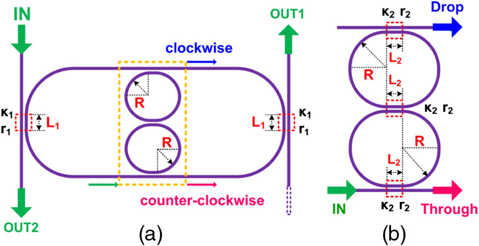
Figure 1.(a) Schematic configuration of the proposed MRR with one NPS. (b) Zoom-in view of NPS marked with dashed box in (a).

Figure 2.(a) Normalized transmission spectrum from IN to OUT1. (b) Normalized transmission spectrum from IN to OUT2. (c) Zoom-in view of (a) and (b) in the wavelength range of 1551.8–1555.8 nm.
The structural parameters are chosen as follows: the gap size in the coupling regions is 0.18 μm, and the straight coupling lengths are and . The radius of each subring is , and the circumference of the outer ring is four times as large as that of each subring. For silicon PWWs with a cross section of , the calculated transmission coefficients of the directional couplers using Lumerical finite-difference time-domain (FDTD) solutions are and . We also assume that the waveguide group index of the transverse electric (TE) mode is and the waveguide transmission loss factor is , which are based on experimental measurements of our previously fabricated devices with the same fabrication process [26]. In Figs. 2(a) and 2(b), one can see that there is a split resonance in a period of wavelength range that covers four free spectral ranges (FSRs) of the outer MRR. The power transmissions at the central wavelengths of the split resonances are lower than those of the unsplit resonances in Fig. 2(a), whereas the power transmissions at the central wavelengths of the split resonances are higher than those of the unsplit resonances in Fig. 2(b); i.e., the extinction ratios at OUT1 and OUT2 are and , respectively. The difference in power transmissions between the split and unsplit resonances can be used to route certain resonance wavelength channels of the outer MRR from OUT1 to OUT2. The intrinsic insertion losses at OUT1 and OUT2 caused by the counter-traveling mode are and , respectively. Due to the additional insertion losses, the power consumption is relatively higher than the WSSs based on MZIs [13] and cascaded MRRs [14]. Stronger coupling between the NPS and the outer MRR, as well as lower loss, would lead to higher extinction ratios between the split and unsplit resonances. The 3 dB bandwidth of the central transmission peak in Fig. 2(c) is , i.e., , which is defined as the processing bandwidth. A larger processing bandwidth could be achieved by increasing the coupling strength between the outer ring and the straight waveguides. An increase in the ratio of the circumference of the outer ring to that of the inner subring would result in a period covering more FSRs, thus leading to an increased number of available wavelength channels that can be handled by a MRR with one NPS. By introducing more NPSs in the outer MRR, the proposed device can be used to selectively route more wavelength channels within the avalaible channels. A WSS can be further implemented by cascading N-1 MRRs with NPS.
3. DEVICE FABRICATION AND MEASURED SPECTRA
The designed devices based on the above principle were fabricated on an 8 in. SOI wafer with a 220-nm-thick top silicon layer and a 2-μm-thick buried dioxide layer. The micrographs of the fabricated devices with one and two NPSs are shown in Figs. 3(a) and 3(b), respectively. The device footprints are and accordingly. The same design parameters were used for the two devices, except that the circumference of the outer ring for the device with two NPSs was six times as large as that of each subring. 248-nm deep ultraviolet (DUV) photolithography was utilized to define the layout, and an inductively coupled plasma (ICP) etching process was used to etch the top silicon layer. Thermo-optic microheaters (TO-MHs) were fabricated along the NPS to tune the central wavelengths of the split resonances without shifting the resonance wavelengths of the outer MRR. Grating couplers for TE polarization were employed at the ends to couple light into and out of the devices with single-mode fibers.
Figure 3.Micrograph of the fabricated devices with (a) one and (b) two NPSs.
The measured transmission spectra from IN to OUT2 and OUT1 of the fabricated device with one NPS are shown in Figs. 4(a) and 4(c), respectively. The on-chip insertion losses at OUT1 and OUT2 are and , respectively. The insertion losses are mainly attributed to the fiber-to-chip coupling loss of induced by the vertical coupling system. The zoom-in spectrum around one of the split resonances at in Fig. 4(a) is fitted by the dashed curve calculated from Eqs. (1) and (2), as shown in Fig. 4(b). The 3 dB bandwidth of the central transmission peak is , which corresponds to a processing bandwidth of . By further increasing the coupling length in the coupling regions, a larger processing bandwidth could be obtained. It can be seen that the measured curve fits well with the simulated one. The fitting parameters are , , , and , which are consistent with our expectations before fabrication. In Fig. 4(a), , , , and denote the central wavelengths of four adjacent resonances of the outer MRR in a wavelength range. The resonance at is split, whereas the resonances at , , and are not. The extinction ratios at OUT1 and OUT2 are and , respectively, which are comparable with the WSSs based on cascaded MRRs in Ref. [14] and slightly lower than the WSSs based on MZIs in Ref. [13]. Increased extinction ratios can be achieved by further optimizing the waveguide transmission loss and the coupling between the NPS and the outer MRR.
Figure 4.(a) Measured transmission spectrum from IN to OUT2 of the fabricated device with one NPS. (b) Zoom-in spectrum around one split resonance at in (a) fitted by the dashed curve calculated from Eqs. (1) and (2). (c)–(f) Measured transmission spectra from IN to OUT1 when the power applied to the microheater is 0.0, 5.8, 11.1, and 16.1 mW, respectively.
By applying a direct-current (DC) voltage to the TO-MH along the NPS, one can selectively block any wavelength channel at OUT1 and route it to OUT2 within a period. When the power applied to the TO-MH is 5.8, 11.1, and 16.1 mW, the measured transmission spectra from IN to OUT1 are shown in Figs. 4(d), 4(e), and 4(f), respectively. There are split resonances at , , and in Figs. 4(d), 4(e), and 4(f), respectively, thus leading to selective channel routing at , , and from OUT1 to OUT2 accordingly. In our experiment, it takes for the split resonances tuning over one FSR of the outer ring to reach a steady state. During the tuning process, the resonance wavelengths of the outer MRR are almost fixed, with a redshift smaller than . The wavelength redshifts are mainly induced by heating crosstalk, which can be compensated by adaptively tuning the resonance wavelengths of the outer ring resonator in a blueshift direction. By electrically tuning the NPS through carrier injection [27], the wavelength redshift can be further reduced.
The measured transmission spectrum from IN to OUT1 of the fabricated device with two NPSs is shown in Fig. 5(a), where denote six adjacent resonance wavelengths of the outer MRR in a wavelength range. There are identical split resonances induced by the two NPSs, thus resulting in channel blocking at with an increased extinction ratio. When the power applied to the TO-MH along one of the two NPSs is 4.5, 8.8, 13.0, 17.0, and 20.7 mW, the measured transmission spectra from IN to OUT1 are shown in Figs. 5(b), 5(c), 5(d), 5(e), and 5(f), respectively. There are split resonances at , , , , and in Figs. 5(b), 5(c), 5(d), 5(e), and 5(f), respectively, allowing for selective channel routing from OUT1 to OUT2 at these wavelengths. The processing bandwidth of the fabricated device with two NPSs is , and the extinction ratios at OUT1 and OUT2 are and , respectively.
Figure 5.Measured transmission spectra from IN to OUT1 of the fabricated device with two NPSs when the power applied to the microheater along one of the two NPSs is (a) 0.0, (b) 4.5, (c) 8.8, (d) 13.0, (e) 17.0, and (f) 20.7 mW, respectively.
4. SYSTEM DEMONSTRATION OF DYNAMIC CHANNEL ROUTING
We use the experimental setup shown in Fig. 6 to test the performance of the fabricated devices as on-chip WSSs. A Mach–Zehnder modulator (MZM) driven by a electrical pseudo random bit sequence (PRBS) signal from a pulse pattern generator (PPG) is used to modulate the continuous-wave (CW) light from a tunable laser. The MZM is biased at the quadrature point of the transmission curve to generate NRZ signal. The generated NRZ signal is amplified by an erbium-doped fiber amplifier (EDFA) followed by a tunable band-pass filter (BPF) to suppress the amplified spontaneous emission (ASE) noise. A polarization controller (PC) is inserted before the device under test (DUT) to make sure that the input signal is TE polarized, followed by an isolator to block the undesired counter-traveling mode. A vertical coupling system is employed to couple light into and out of the DUT. The signal output from the DUT is split into two parts by a fiber splitter. One part is fed into an optical spectrum analyzer (OSA), and the other is amplified by another EDFA and passes through a second BPF to suppress the ASE noise before finally being sent to an oscilloscope.
Figure 6.Experimental setup for system demonstration of dynamic channel routing using the fabricated device. VOA, variable optical attenuator.
When the wavelength of the CW light is set to , , , and in Fig. 4(a), the eye diagrams of the signal output from OUT1 are shown in Fig. 7(a-I) accordingly. The input NRZ signal is blocked at due to resonance splitting, and one cannot observe the opened eye diagram at this wavelength channel. When the power applied to the TO-MH is 5.8, 11.1, and 16.1 mW, the input NRZ signal is blocked at , , and with closed eye diagrams observed, respectively. On the other hand, the eye diagrams of the signal output from OUT2 when the wavelength of the CW light is set to , , , and in Fig. 4(a) are shown in Fig. 7(a-II). The wavelength channel at is routed to OUT2 with an opened eye diagram, whereas it is blocked at , , and with closed eye diagrams. By tuning the power applied to the TO-MH along the NPS, the wavelength channels at , , and can be routed to OUT2 with opened eye diagrams observed. Similarly, the eye diagrams of NRZ signal output from OUT1 and OUT2 of the fabricated device with two NPSs are shown in Figs. 7(b-I) and 7(b-II), respectively. By tuning the power applied to the TO-MH along one of the two NPSs, the wavelength channels at , , , , and can be selectively routed to OUT2. The wavelength channel at remains blocked at OUT1 since it is routed to OUT2 by the other NPS without being thermally tuned. All four sets of experimental results in Fig. 7 verify the effectiveness of the fabricated devices as on-chip WSSs routing up to six wavelength channels. The BER curves measured with the fabricated devices with one and two NPSs are shown in Figs. 8(a) and 8(b), respectively. The power penalties are and at OUT1/OUT2 of the fabricated devices with one and two NPSs, respectively. Based on these experimental results, it can be concluded that the proposed devices could be used to selectively route multiple wavelength channels within a period.
Figure 7.Eye diagrams of NRZ signal output from (a-I) OUT1 and (a-II) OUT2 of the fabricated device with one NPS at wavelengths of when the heating power is 0.0, 5.8, 11.1, and 16.1 mW, respectively. Eye diagrams of NRZ signal output from (b-I) OUT1 and (b-II) OUT2 of the fabricated device with two NPSs at wavelengths of when the heating power is 0.0, 4.5, 8.8, 13.0, 17.0, and 20.7 mW, respectively.
Figure 8.BER curves measured with the fabricated devices with (a) one and (b) two NPSs.
5. CONCLUSION
In conclusion, we have proposed and experimentally demonstrated compact on-chip WSSs based on silicon MRRs with NPSs. The proposed devices can be used to perform selective channel routing at certain resonance wavelengths of the outer MRRs without affecting the others. Extinction ratios over 16 dB and processing bandwidths over 25 GHz are experimentally measured with the fabricated devices. The peformance of the fabricated devices with one and two NPSs as effective WSSs has also been tested through a system experiment with NRZ signal. The compact footprint, CMOS compatibilty, and flexibility in controlling the resonance attributes suggest that the proposed devices could be functional components in future WDM optical communication networks.
References
[1] T. Strasser, J. Wagener. Wavelength-selective switches for ROADM applications. IEEE J. Sel. Top. Quantum Electron., 16, 1150-1157(2010).
[2] N. Kataoka, N. Wada, K. Sone, Y. Aoki, H. Miyata, H. Onaka, K. Kitayama. Field trial of data-granularity-flexible reconfigurable OADM with wavelength–packet-selective switch. J. Lightwave Technol., 24, 88-94(2006).
[3] J. Rhee, I. Tomkos, M. Li. A broadcast-and-select OADM optical network with dedicated optical-channel protection. J. Lightwave Technol., 21, 25-31(2003).
[4] E. Basch, R. Egorov, S. Gringeri, S. Elby. Architectural tradeoffs for reconfigurable dense wavelength-division multiplexing systems. IEEE J. Sel. Top. Quantum Electron., 12, 615-626(2006).
[5] R. Shankar, M. Florjanczyk, T. Hall, A. Vukovic, H. Hua. Multi-degree ROADM based on wavelength selective switches: architectures and scalability. Opt. Commun., 279, 94-100(2007).
[6] G. Nielson, D. Seneviratne, F. Lopez-Royo, P. Rakich, Y. Avrahami, M. Watts, H. Haus, H. Tuller, G. Barbastathis. Integrated wavelength-selective optical MEMS switching using ring resonator filters. IEEE Photon. Technol. Lett., 17, 1190-1192(2005).
[7] D. Marom, D. Neilson, D. Greywall, C. Pai, N. Basavanhally, V. Aksyuk, D. López, F. Pardo, M. Simon, Y. Low, P. Kolodner, C. Bolle. Wavelength-selective 1×K switches using free-space optics and MEMS micromirrors: theory, design, and implementation. J. Lightwave Technol., 23, 1620-1630(2005).
[8] B. Fracasso, J. Tocnaye, M. Razzak, C. Uche. Design and performance of a versatile holographic liquid-crystal wavelength-selective optical switch. J. Lightwave Technol., 21, 2405-2411(2003).
[9] J. Ertel, R. Helbing, C. Hoke, O. Landolt, K. Nishimura, P. Robrish, R. Trutna. Design and performance of a reconfigurable liquid-crystal-based optical add/drop multiplexer. J. Lightwave Technol., 24, 1674-1680(2006).
[10] K. Suzuki, T. Mizuno, M. Oguma, T. Shibata, H. Takahashi, Y. Hibino, A. Himeno. Low loss fully reconfigurable wavelength-selective optical 1×N switch based on transversal filter configuration using silica-based planar lightwave circuit. IEEE Photon. Technol. Lett., 16, 1480-1482(2004).
[11] M. Earnshaw, M. Cappuzzo, E. Chen, L. Gomez, A. Griffin, E. Laskowski, A. Wong-Foy. Highly-integrated planar lightwave circuit wavelength selective switch. Electron. Lett., 39, 1397-1398(2003).
[12] W. Bogaerts, P. Dumon, D. Van Thourhout, D. Taillaert, P. Jaenen, J. Wouters, S. Beckx, V. Wiaux, R. Baets. Compact wavelength-selective functions in silicon-on-insulator photonic wires. IEEE J. Sel. Top. Quantum Electron., 12, 1394-1401(2006).
[13] C. Doerr, L. Buhl, L. Chen, N. Dupuis. Monolithic gridless 1 × 2 wavelength-selective switch in silicon. Proc. OFC, PDPC4(2011).
[14] Y. Goebuchi, M. Hisada, T. Kato, Y. Kokubun. Optical cross-connect circuit using hitless wavelength selective switch. Opt. Express, 16, 535-548(2008).
[15] Y. Zhang, Y. Li, S. Feng, A. W. Poon. Towards adaptively tuned silicon microring resonators for optical networks-on-chip applications. IEEE J. Sel. Top. Quantum Electron., 20, 5900514(2014).
[16] P. Dong, S. Preble, M. Lipson. All-optical compact silicon comb switch. Opt. Express, 15, 9600-9605(2007).
[17] Y. Wen, O. Kuzucu, M. Fridman, A. Gaeta, L. Luo, M. Lipson. All-optical control of an individual resonance in a silicon microresonator. Phys. Rev. Lett., 108, 223907(2012).
[18] L. Zhang, M. Song, T. Wu, L. Zou, R. Beausoleil, A. Willner. Embedded ring resonators for microphotonic applications. Opt. Lett., 33, 1978-1980(2008).
[19] X. Zhou, L. Zhang, A. Armani, R. Beausoleil, A. Willner, W. Pang. Power enhancement and phase regimes in embedded microring resonators in analogy with electromagnetically induced transparency. Opt. Express, 21, 20179-20186(2013).
[20] L. Barea, F. Vallini, G. de Rezende, N. Frateschi. Spectral engineering with CMOS compatible SOI photonic molecules. IEEE Photon. J., 5, 2202717(2013).
[21] L. Barea, F. Vallini, P. Jarschel, N. Frateschi. Silicon technology compatible photonic molecules for compact optical signal processing. Appl. Phys. Lett., 103, 201102(2013).
[22] Z. Zhang, M. Dainese, L. Wosinski, M. Qiu. Resonance-splitting and enhanced notch depth in SOI ring resonators with mutual mode coupling. Opt. Express, 16, 4621-4630(2008).
[23] M. Souza, L. Barea, F. Vallini, G. Rezende, G. Wiederhecker, N. Frateschi. Embedded coupled microrings with high-finesse and close-spaced resonances for optical signal processing. Opt. Express, 22, 10430-10438(2014).
[24] J. Wu, T. Pan, P. Cao, X. Hu, L. Jiang, X. Jiang, Y. Su. Compact wavelength blocker based on silicon microring resonator with nested pair of subrings. Proc. OECC/ACOFT, TU4E-2(2014).
[25] A. Yariv. Critical coupling and its control in optical waveguide-ring resonator systems. IEEE Photon. Technol. Lett., 14, 483-485(2002).
[26] J. Wu, P. Cao, X. Hu, T. Wang, M. Xu, X. Jiang, F. Li, L. Zhou, Y. Su. Nested configuration of silicon microring resonator with multiple coupling regimes. IEEE Photon. Technol. Lett., 25, 580-583(2013).
[27] L. Zhou, A. W. Poon. Electrically reconfigurable silicon microring resonator-based filter with waveguide-coupled feedback. Opt. Express, 15, 9194-9204(2007).


