Author Affiliations
1State Key Laboratory of Transducer Technology, Shanghai Institute of Technical Physics, Chinese Academy of Sciences, Shanghai 200083, China2Shanghai Institute of Microsystem and Information Technology, Chinese Academy of Sciences, Shanghai 200050, Chinashow less
The heteroepitaxy of semiconductor thin films is a cornerstone of semiconductor devices and is naturally preferred to grow on matched substrates from the view point of material epitaxy. However, the heteroepitaxy is always performed on mismatched substrates due to the limited choices of mature substrates, which constrains the quality of semiconductor thin films. In past decades, numerous metamorphic buffer layers and pre-growth processing have been developed to control the defect density in the epitaxial semiconductor thin films on heterogeneous mismatched substrates. Through these approaches, some kinds of semiconductor lasers, detectors and electronic devices with high performances have been achieved and applied in industry. However, people are always keeping a dream to epitaxially grow high quality semiconductor thin films on arbitrary substrates. The heteroepitaxy through two-dimensional (2D) materials could be a potential route. If one can grow sp3-bonded three-dimensional (3D) epitaxial films on 2D materials, the limitation of matched substrates will be overcome. Furthermore, the transfer of single-crystalline semiconductor thin films will be allowed due to the weak van der Waals interaction.
High quality GaN thin films with low threading dislocations and light emitting diodes (LEDs) with high performances and flexibility have been demonstrated on many substrates through graphene and other 2D materials, causing the researches on this topic grow rapidly[1, 2]. The interfacial buffers or artificial treatments are usually employed for the heteroepitaxy to achieve periodic nucleation sites between the 3D and 2D materials. Then there comes a question whether other semiconductor thin films, e.g. another widely used III–V semiconductor GaAs, are able to grown on mismatched substrates through 2D materials. The answer is: possible but difficult.
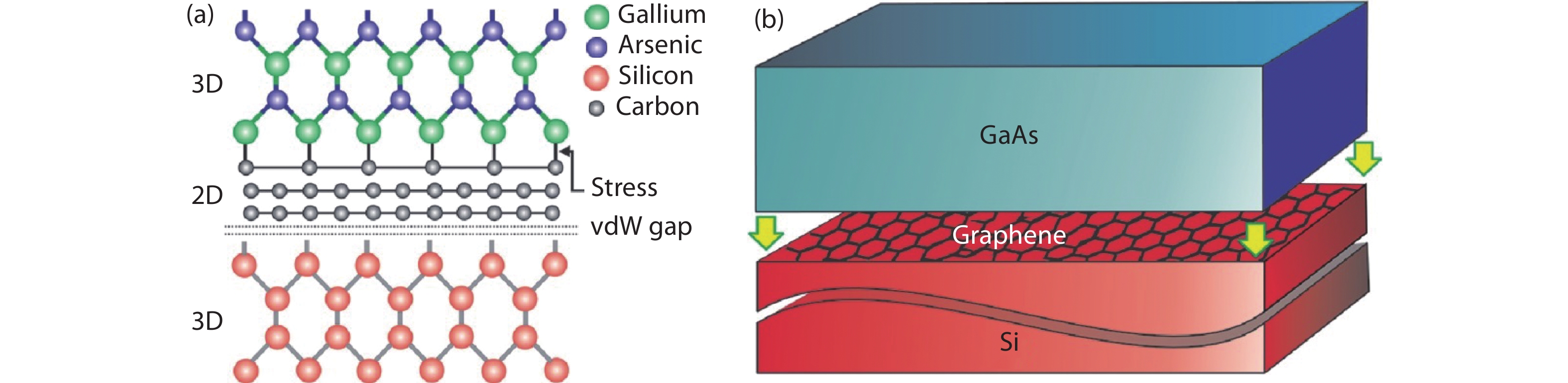
Although a number of studies have been undertaken to achieve high quality GaAs nanowire on graphene, the single-crystalline thin films are attractive to demonstrate high performance devices. In 2014, Alaskar et al.reported GaAs single-crystalline thin films with smooth morphology on Si substrate through multilayer graphene as shown in Fig. 1[3]. From their theoretical calculation, the 2D growth of III–arsenide films encounters much larger challenges than III–nitrides due to the much lower adsorption and migration energy as well as lower ratio of adsorption energy to bulk cohesive energy for III–arsenides. The smooth GaAs single-crystalline thin films were grown on multiplayer graphene/Si by using Ga-prelayer and delicately controlled growth temperature. In 2017, Kim et al. reported that GaAs homoepitaxial single-crystalline films was able to achieve on GaAs substrates through monolayer graphene, and an epitaxial alignment of Ga atoms to As atoms was found, which is also applicable to the cases of InP and GaP[4]. The so-called “remote epitaxy” technique enables the copy of semiconductor films from underlying substrates and is attractive in the re-using of graphene-coated substrates. More recently, the effects of polarity on the remote epitaxy of semiconductor thin films on 2D material coated substrates are investigated, and the types of single-crystalline thin films suitable for this technique are predicted by Kong et al.[5]. The potential field from ionic-bonded materials was found strong enough topenetrate through a few layers of graphene. They claimed that for the lattice mismatched system of GaN-GaAs, the nuclei-substrate interaction did not increase with the size of nuclei, and the enhancement of potential energy fluctuation was prevented by the mismatch-induced broad distribution of local dipole alignments.
![(Color online) (a) Schematic atomic geometry and (b) schematic epitaxial structure of GaAs thin film on graphene-coated Si substrate[3].](/Images/icon/loading.gif)
Figure 1.(Color online) (a) Schematic atomic geometry and (b) schematic epitaxial structure of GaAs thin film on graphene-coated Si substrate[3].
In the case of semiconductor thin films epitaxially grown on mismatched substrates, the use of metamorphic buffer is still, and will be for a long time, the main route for mass production. However, the heteroepitaxy through 2D material buffer is very attractive. Recent advances have confirmed the possibility of this promising route, while following main questions need to be further addressed:
1) The applicable nucleation sites for the heteroepitaxy of different semiconductor thin films. Defects of 2D materials, nanowire structures, potential field of substrates, or others?
2) The effects of different 2D materials and substrates, including the layer number of 2D materials, the acquisition and pre-growth treatment methods of 2D materials, etc.
3) The interaction of epitaxial 3D thin films with local 2D materials. The alloy atoms as well as dislocations, stacking faults and other crystal defects all need to be considered.
References
[1] K Chung, C H Lee, G C Yi. Transferable GaN layers grown on ZnO-coated graphene layers for optoelectronic devices. Science, 330, 655(2010).
[2] J Kim, C Bayram, H Park et al. Principle of direct van der Waals epitaxy of single-crystalline films on epitaxial graphene. Nat Commun, 5, 4836(2014).
[3] Y Alaskar, S Arafin, D Wickramaratne et al. Towards van der Waals epitaxial growth of GaAs on Si using a graphene buffer layer. Adv Funct Mater, 24, 6629(2014).
[4] Y Kim, S Cruz, K Lee et al. Remote epitaxy through graphene enables two-dimensional material-based layer transfer. Nature, 544, 340(2017).
[5] W Kong, H Li, K Qiao et al. Polarity governs atomic interaction through two-dimensional materials. Nat Mater, 17, 999(2018).