Abstract
Miniaturized spectrometers have been widely researched in recent years, but few studies are conducted with on-chip multimode schemes for mode-division multiplexing (MDM) systems. Here we propose an ultracompact mode-division demultiplexing spectrometer that includes branched waveguide structures and graphene-based photodetectors, which realizes simultaneously spectral dispersing and light fields detecting. In the bandwidth of 1500–1600 nm, the designed spectrometer achieves the single-mode spectral resolution of 7 nm for each mode of TE1–TE4 by Tikhonov regularization optimization. Empowered by deep learning algorithms, the 15-nm resolution of parallel reconstruction for TE1–TE4 is achieved by a single-shot measurement. Moreover, by stacking the multimode response in TE1–TE4 to the single spectra, the 3-nm spectral resolution is realized. This design reveals an effective solution for on-chip MDM spectroscopy, and may find applications in multimode sensing, interconnecting and processing.Miniaturized spectrometers have been widely researched in recent years, but few studies are conducted with on-chip multimode schemes for mode-division multiplexing (MDM) systems. Here we propose an ultracompact mode-division demultiplexing spectrometer that includes branched waveguide structures and graphene-based photodetectors, which realizes simultaneously spectral dispersing and light fields detecting. In the bandwidth of 1500–1600 nm, the designed spectrometer achieves the single-mode spectral resolution of 7 nm for each mode of TE1–TE4 by Tikhonov regularization optimization. Empowered by deep learning algorithms, the 15-nm resolution of parallel reconstruction for TE1–TE4 is achieved by a single-shot measurement. Moreover, by stacking the multimode response in TE1–TE4 to the single spectra, the 3-nm spectral resolution is realized. This design reveals an effective solution for on-chip MDM spectroscopy, and may find applications in multimode sensing, interconnecting and processing.Introduction
To cope with the ever-growing shortage of communication resources, advanced multiplexing technologies such as wavelength-division multiplexing (WDM)1 and polarization-division multiplexing (PDM), have been developed to realize multi-channel parallel data transmissions. In the past decades, mode-division multiplexing (MDM) technology has attracted considerable attention2, 3, 4, which divides mutually orthogonal mode channels in a single wavelength. Various kinds of multimode manipulating and processing devices have been springing up, such as mode multiplexers/demultiplexers5, 6, mode converters7–9, and mode switches10. Due to the lack of devices that simultaneously integrate the functions of mode demultiplexing and spectral measurement, the sophisticated photo-detecting circuits are usually required when extracting the wavelength-dependent information carried on independent modes11, 12. Moreover, to the best of our knowledge, none of related works consider high-order modes as individual channels to directly recognize multiple spectra from separated sources. Therefore, the on-chip multimode spectrometers compatible in MDM systems still remain an open problem.
Optical spectroscopy is a ubiquitous technique from scientific research to engineering practices. In witness of innovative miniaturized optical spectrometers on silicon-on-insulator (SOI) platforms13, spectroscopic analysis has become more convenient for the specific applications that usually require real-time and comparable results rather than ultra-high accuracy, including instantaneous biosensing14, 15, mobile spectral imaging16–18, and signal monitoring for coherent optical communications19, 20. Spectrometers generally contain the wavelength-selective elements and photodetection components. Recently, the miniaturized spectrometers based on gradient-bandgap nanowires or tunable two-dimensional (2D) materials have realized the integration of material-based dispersion and photoelectric detection21, 22, which are operated with free-space light illumination. For on-chip waveguide-integrated spectrometers, the usual approach is to combine the narrowband filters or interferometers with a single photodetector or multiple photodetectors, which increases the spectrometer footprint and restricts denser integration23. To realize the ultimate multimode spectrometers in MDM systems, we argue that the novel design of spectral dispersive components and broadband photodetecting elements are required. Moreover, the advanced reconstruction algorithms are in demand to deal with the strong nonlinear coupling effects between various modes. The fast development of deep learning (DL) techniques merging with photonics may shed new light on this difficulty24-30. DL offers high plasticity to nonlinear optimizations and complicated tasks, whose target functions are difficult to express or solve by conventional optimization methods, such as compressive sensing31-33 and regularization-based algorithms34-36. In addition, because of the end-to-end training manner, it is unnecessary for DL-empowered reconstructions to know the physical properties of devices in advance, supporting a transferable architecture for the multimode spectrometers.
In this work, we for the first time propose an on-chip mode-division demultiplexing (MDD) compatible spectrometer with deep learning. The ultracompact multimode spectrometer in footprint of 63×12 μm2 (estimated based on simulation) integrates a highly branched waveguide along with an array of coupled graphene photodetectors, which realize simultaneously spectral dispersing and light fields detecting. In the bandwidth of 1500–1600 nm, the designed spectrometer achieves the single-mode spectral resolution of 7 nm for each mode of TE1–TE4 by Tikhonov regularization optimization21, 37, 38. Besides, the deep learning algorithms are implemented to tackle the strong mode coupling effects in multimode demultiplexing, and the 15 nm resolution of parallel reconstruction for TE1-TE4 is achieved by the single-shot measurement. Moreover, we investigate the spectral resolution enhancement technique by stacking multi-shot multimode measurement, and an average resolution of 3 nm is achieved. Our work provides an effective way for MDM spectroscopy that may find applications in multimode sensing, interconnecting and processing, with benefits for future on-chip dense integrations.
Results
Device design and Tikhonov regularization-based reconstruction
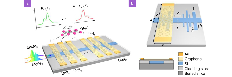
A simplified schematic of the proposed MDD spectrometer on SOI platform is illustrated in Fig. 1(a), which consists of a backbone multimode branched waveguide and m 2D-material-based photodetecting units, i.e., unit1–unitm. Here, 2D materials, such as graphene and black phosphorus, can be selected as the photodetecting layer due to their advantages in flexible integration and broad operation wavelength range39. For example, graphene has the potential for high-speed and broadband photodetection thanks to its gapless bandstructure and high carrier mobility40, 41, 42. The small direct bandgap of black phosphorus makes it advantageous for infrared spectra detection39. 2D materials meet the imperative demand of on-chip photonics for high-performance and broadband photodetectors. As a proof-of-concept study, we consider the photoconductive effect of the metal−graphene−metal photodetectors43-46. In a photoconductive device, photon absorption generates extra free carriers, reducing the electrical resistance of the semiconductor. The evanescent fields of the waveguide enhance the light-graphene interactions. The incident photons cause the change of the channel electrical conductivities, and the photocurrents can be extracted by applying a bias voltage39. The magnitude of the photocurrent is proportional to the material’s absorption (more details see Supplementary information Section S1). The highly branched structures of silicon waveguide integrated with the transparent graphene photodetectors realize simultaneously spectral dispersing and light fields detecting. In particular, when the multimode spectra carried on k guided modes, i.e., mode1–modek, are launched from the input port, the photocurrents I1–Im in the graphene photodetecting units are generated. Then the captured photocurrent arrays are fed into a deep neural network (DNN) to separate and rebuild the desired spectral profiles F1 (λ)–Fk(λ) corresponding to mode1-modek, where λ is light wavelength. In Fig. 1(b), each detecting unit, which occupies an area of x×y, is made of several branched stripes symmetrically assigned on both sides of the backbone waveguide with width w, and a monolayer graphene laminating on the top. Inspired by ref.23, each branched waveguide is determined by parameters (s, h, g). In addition, the gap between adjacent detectors and the thickness of silicon layer are defined as d and t respectively. Comprehensive research is carried out when selecting design parameters. After trying x in the range of 1–3 μm and y in the range of 4–12 μm, we finally fix x=1.5 μm and y=12 μm. In order to achieve the balance between the number of supported modes and the wavelength sensitivity, the width of backbone waveguide w is set as 3 μm. Moreover, m is set as 25 because the resolution is slightly improved as m is larger than 25. We set d=1 μm, t=220 nm, and randomly select parameters (s, h, g) to mimic random medium, where s ∈ [180, 390] nm, h ∈[180, 4200] nm, and g ∈[180, 300] nm. Specifically, mode1–modek are set as TE1–TE4. Note that TE0 mode is unused under the current design parameters, due to its insensitivity to branched microstructures and the much smaller spectral response fluctuations than those of TE1–TE4 (Supplementary Fig. S1). More information about the influences of the design parameters are offered in Supplementary information Section S2. The effective footprint of the multimode spectrometer is as small as 63×12 μm2 estimated based on the simulations. For the graphene photodetectors, a thin SiO2 layer (10 nm) deposited on the planarized chip electrically isolates the graphene layer from the underlying silicon structures, which minimizes the impact of the silicon branching structure on the detector’s performance. The propagating light fields are absorbed by the graphene layer through the evanescent field coupling, leading to the generation of photocarriers. The spectral responsivity at uniti for kth mode can be expressed by47:
, where Di is the area of graphene photodetecting uniti, and
is the simulated electric field for kth mode in the graphene layer. Two metal electrodes located on opposite sides of the waveguide collect the photocurrent. In order to pursue high spectral resolution and waveguide-mode discrimination, it is required for high dissimilarity of spectral responses of varied modes, which can be evaluated by the condition number of their matrix form48. Generally speaking, the lower condition number indicates the higher dissimilarity. To evaluate the overall dissimilarity, we define
as the average of the condition numbers corresponding to TE1-TE4, where Akis the spectral response matrix for kth mode, and
is the condition number of Ak. More details can be found in Supplementary information Fig. S3. Since the shapes of waveguides and the selection of guided modes affect the distribution of effective indices and optical fields, the spectral diversity of unit1–unitm is actually determined by the branched structural parameters as well as waveguide mode group.

Figure 1.(a) Illustration of the proposed mode-division demultiplexing (MDD) spectrometer. The multimode spectral signal (mode1–modek) dispersed in the branched waveguide structures and detected by graphene-photodetector units. The generated photocurrents I1–Im at unit1–unitm from the input multimode spectral signals are fed into a deep neural network (DNN) to extract the desired spectral profiles F1 (λ)–Fk(λ). (b) Structural parameters of a designed branched waveguide and graphene photodetector. Inset: the cross-section view of a silicon waveguide and graphene photodetector.
Through three-dimensional finite-difference time-domain simulations and structural optimizations, the integrated structure with the lowest averaged condition number (cond=1667) is eventually chosen for the spectral range of 1500–1600 nm. The normalized spectral responses for TE1–TE4 at two typical photodetecting unit5 and unit20 are shown in Fig. 2(a). More information about the detecting units and design parameters are provided in Supplementary information Section S2. It is observed that the spectral response at a photodetector behaves quite dissimilarly for different waveguide modes. Furthermore, the light field with higher-order mode is, in general, more sensitive to the variation of refractive index distribution of the branched waveguides, leading to stronger fluctuation than that with lower-order mode. Note that the transmission attenuates gradually because of the light scattering and absorption of the composite waveguides, which sets the fundamental limit of the number of cascading units.
Figure 2.Simulated characterizations of the proposed device for the single-mode (TE1–TE4) spectrometer by Tikhonov regularization optimization. (a) Normalized photoresponses of two typical spectral detecting units. (b) Correlation functions of the spectral responses for different TE modes. (c, d) Recovered spectral profiles of dual peaks separated by 7 nm (c) and the same random spectra (d) for TE1–TE4.
The resolution for a single-mode spectral input is first estimated. The spectral correlation function for each mode (TE1–TE4) is calculated by49:
Note that the correlation function of each mode is averaged over 25 detecting units. Overall, the full width at half-maximum (FWHM) of
is ~7 nm for each mode, which implies the spectral resolution of 7 nm, as is shown in Fig. 2(b). Next, to verify the performance of the designed structures, the simulated photocurrent Ii,k at uniti with kth-mode input is given by:
where
and
specify the bandwidth range. By decomposing Fk(λ) into Gaussian basis expansion, the reconstruction task can be transferred into a problem to find out the optimal weights of Gaussian bases, i.e.,
, to fit the following equation:
where
is an m×n matrix for kth mode with elements equal to the integrals of spectral response and Gaussian basis function, and
is the vector of simulated currents for kth mode. Tikhonov regularization optimization is implemented to search for the optimal
(more details see Supplementary information Section S3). In Fig. 2(c), dual spectral peaks separated by 7 nm in wavelength can be resolved when the light fields with any one of TE1–TE4 is input to the spectrometer. The mean square error (MSE) between reconstructed profile and ground-truth spectrum is regarded as the quantification criteria to evaluate the reconstruction precision. Due to the MSE of 1000 random spectra as low as 0.0004 and the high overlap with the reference curve in Fig. 2(d), the recovered spectral envelopes of the same random spectra further show the generalization capability for single-mode reconstruction over the operating bandwidth.
Single-shot multimode spectral reconstruction
Although the aforementioned optimization method is helpful for single-mode spectral reconstruction, it is still challenging to formulate or solve complex simultaneous multi-mode problems, such as demultiplexing and rebuilding multiple single-mode spectra from a multimode spectra input in a single shot. To cope with this difficulty, a single-shot multimode reconstruction (SMR) computational framework is proposed here. As shown in Fig. 3, the multimode target spectra (F1 (λ)–Fk(λ)), are separately modulated into mode1-modek and imported together with the proposed MDD spectrometer, exciting the multimode interference electric fields at unit1–unitmwhich can be expressed as
, where
is the spectra-dependent electric field with regard to modelin the detection unitDi. The response currents I1–Imcaused by evanescent field coupling are obtained by
. Here, the photoresponse depends substantially on the wavelength and mode state of the input light fields, which enables using DNN to achieve the multimode spectroscopy analysis. Due to end-to-end manner driven by data, once the size of training dataset is sufficient, and the dissimilarity, which can also be called diversity, of the samples ensures that the current-to-spectrum mapping under nonlinear coupling effect is stable and distinguishable, and thus DNN will be effective for the analysis. The generated photocurrents I1–Imas the format of a pixel imageare subsequently fed into the SMR-DNN model to implement simultaneous reconstruction of multimode spectra in single shot. To learn the statistical relationship between the images and target spectra, the major components of SMR-DNN consist of convolutional neural networks (CNN) and fully-connected layers (FC). In essence, CNNs are used to extract invariant features from images, while FCs are used for learning the nonlinear mapping from features to target spectra. A dropout layer is embedded between the FCs to prevent overfitting and improve generalization ability.
Figure 3.Principle of the single-shot multimode reconstruction (SMR) algorithm. The unknown multimode spectra are imported to the proposed MDD spectrometer at the same time. The response photocurrents I1-Imare captured at unit1-unitm, and then are fed into the trained SMR-DNN as a pixel image to implement simultaneous reconstruction of different mode spectra in single shot.
The SMR-DNN model is trained to reconstruct the spectra of TE1–TE4 modes with 25 detectors. The input is made of 5×5 pixels by pixelating I1–I25. The output has 404 data points by joining four mode-spectra (TE1–TE4), and the single-mode spectra are represented by 101 data points. After 200 epochs by the Adam optimizer, the testing MSE eventually reaches 0.0017. More details about the setup and training procedure of SMR-DNN are offered in Supplementary information Section S4. Figure 4 shows the single-shot rebuilding capability of the trained model. From Fig. 4(a, b), the resolvable FWHM of optical spectral reaches 15 nm. When the parallel reconstruction is implemented, dual peaks at 15-nm intervals are successfully distinguished, and meanwhile, single peaks with 15 nm FWHM uniformly distributed in the bandwidth can be largely fitted. In addition, in Fig. 4(c–f), four random spectra loaded on TE1–TE4 are well recognized (MSE=0.0015), which proves the ability of parallel reconstruction. In addition, these results also show the effectiveness of DL techniques for the nonlinear optimization problems. Such design not only significantly reduces the number of optical elements and the space occupation at the receiver end of MDM multi-sensor networks, but also can be utilized for online monitoring of MDM communication quality. To the best of our knowledge, the MDD spectrometer is for the first time proposed to realize the simultaneous multimode spectra construction in a single shot, which is fully compatible to the current MDM system. Although the current designed resolution of the MDD spectrometer is not high, it is promising to improve the resolution by optimizing both the dispersive photonic structures and photodetecting materials.
Figure 4.Single-shot simultaneous multimode reconstructions from the trained SMR-DNN for TE1–TE4. (a) Dual spectral peaks resolution with light wavelength separated by 15 nm, (b) single peaks with FWHM-15 nm uniformly distributed in the bandwidth of 1500-1600 nm. (c–f) The construction of multimode spectra in different modes: (c) TE1, (d) TE2, (e) TE3, and (f) TE4.
Multi-shot resolution-enhanced spectral reconstruction
In this section, we discuss the potential of improving the spectral resolution of a single-mode by harnessing the multi-mode dispersing effect. In particular, a multi-shot resolution-enhanced (MRE) architecture is designed to strengthen resolving ability in multiple shots, which is presented in Fig. 5(a). Target spectra are individually modulated into mode1–modek in temporal slices T1–Tk, generating k images of pixelated single-mode currents. The modulation operation can be implemented by reconfigurable mode converters7, 8. After that, the samples composed of these k images are input into MRE-DNN to achieve resolution enhancement. As a proof of concept, TE1–TE4 are selected as the carriers to transmit the target spectra in T1–T4 separately. The input of MRE-DNN is with a size of 4×5×5 corresponding to 5×5 pixelated currents in 4-mode channels, while the spectral output is represented more precisely by 1010 data points. The testing MSE finally stops at 0.0007 after 200 epochs, and more information about MRE-DNN is provided in Supplementary information Section S4. Figure 5(b, c) display the reconstructed spectral results, confirming a stable FWHM-3 nm resolution over the bandwidth of 1500–1600 nm, which is ~1.3 times higher than that of Tikhonov regularization-based method. The rebuilding power for random spectra over the operating bandwidth is also well realized as shown in Fig. 5(d). Notably, if the number of implemented modes is increased, the spectral resolution is expected to be further improved.
Figure 5.Principle and performance of the designed multi-shot resolution-enhanced (MRE) architecture. (a) Principle of the MRE algorithm. The various single-mode photocurrent (T1–Tk) images are generated by the spectral responses of photodetecting arrays and are fed into MRE-DNN to obtain resolution-improved results. (b–d) Recovered results of dual spectral peaks with light wavelength separated by 3 nm (b), single peaks with FWHM-3 nm uniformly distributed in the bandwidth (c), and the constructed random spectra (d).
Conclusion
In summary, we propose an ultracompact MDD spectrometer that integrates a highly branched multimode waveguide and 25 graphene-based photodetectors on SOI platform. In the bandwidth of 1500–1600 nm, the simulation results show that it can realize the single-mode spectral resolution of 7 nm for each mode of TE1–TE4 by Tikhonov regularization optimization. Empowered by DL algorithms, the 15-nm resolution of parallel reconstruction for TE1–TE4 is obtained by SMR framework. Moreover, by stacking the multimode response to the single spectra in TE1–TE4, the MRE architecture shows ~3 nm resolution, which is ~1.3 times improvement compared to Tikhonov regularization-based method. For practical applications, considering the existence of manufacturing tolerances and measurement deviations from the designed structures, it is necessary to modify the simulation structures and recalibrate the spectral responses to ensure the consistency between simulations and experiments. Adequate training samples should be regenerated based on the modified structures to update the DNNs. Together with the dissimilarity of the training samples and the noise robustness of DNN, it is reasonable to believe that the simulation results can be compared with the future experimental demonstrations. The fusion of optical mode demultiplexing and spectral detection functions in a single device is proposed here for the first time, and it provides a feasible way for miniaturization and integration of optical spectrometers. More importantly, it reveals more usages of guided modes, which sheds light on new spectroscopic architectures for MDM systems.
Acknowledgements
This project was supported by the National Natural Science Foundation of China (Grants No. 62005231), Fundamental Research Funds for the Central Universities (20720210045, 20720200074) and Guangdong Basic and Applied Basic Research Foundation (2021A1515012199).
The authors declare no competing financial interests.
Supplementary information for this paper is available at https://doi.org/10.29026/oes.2022.220012