• Acta Optica Sinica
  • Vol. 42, Issue 1, 0131001 (2022)
Mengke Zheng1、2, Jie Li2, Rongzhu Zhang1、**, and Liqun Chai2、*
Author Affiliations
  • 1College of Electronics and Information Engineering, Sichuan University, Chengdu, Sichuan 610064, China
  • 2Research Center of Laser Fusion, China Academy of Engineering Physics, Mianyang, Sichuan 621900, China
  • show less
    DOI: 10.3788/AOS202242.0131001 Cite this Article Set citation alerts
    Mengke Zheng, Jie Li, Rongzhu Zhang, Liqun Chai. Analysis and Simulation on Damage Characteristics of Multilayer Optical Film by Pulsed Laser[J]. Acta Optica Sinica, 2022, 42(1): 0131001 Copy Citation Text show less
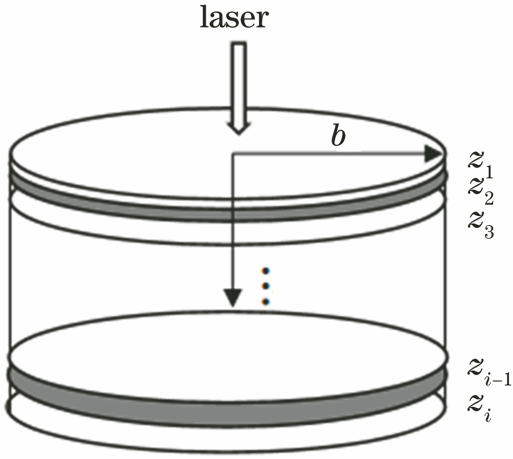
    Analysis model of multilayer film irradiated by laser
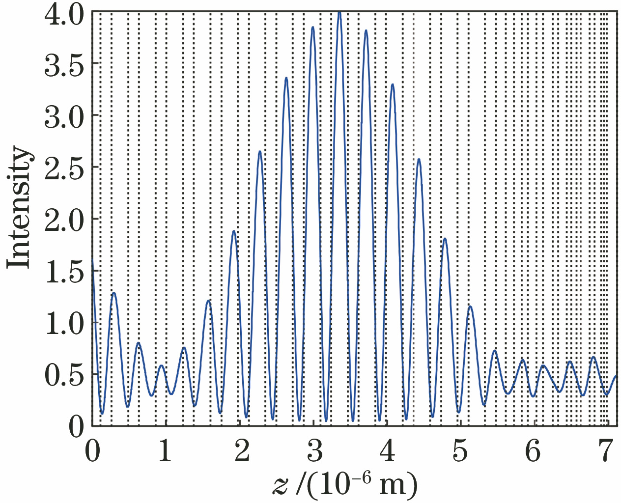
    Fig. 1. Analysis model of multilayer film irradiated by laser
    Standing wave field distribution in multilayers
    Fig. 2. Standing wave field distribution in multilayers
    Temperature distribution in film under incidence of pulse with pulse width of 10 ns. (a) Temperature at center of film; (b) curve of temperature peak with time
    Fig. 3. Temperature distribution in film under incidence of pulse with pulse width of 10 ns. (a) Temperature at center of film; (b) curve of temperature peak with time
    Spatial distribution of stress field in film under incidence of pulse with pulse width of 10 ns. (a) Radial stress; (b) annular stress; (c) axial stress
    Fig. 4. Spatial distribution of stress field in film under incidence of pulse with pulse width of 10 ns. (a) Radial stress; (b) annular stress; (c) axial stress
    Maximum stress field distribution of film under incidence of pulse with pulse width of 10 ns. (a) HfO2 film layer; (b) SiO2 film layer
    Fig. 5. Maximum stress field distribution of film under incidence of pulse with pulse width of 10 ns. (a) HfO2 film layer; (b) SiO2 film layer
    Change of photon ionization rate in film under incidence of pulse with pulse width of 10 ns. (a) Avalanche ionization rate; (b) multiphoton ionization rate
    Fig. 6. Change of photon ionization rate in film under incidence of pulse with pulse width of 10 ns. (a) Avalanche ionization rate; (b) multiphoton ionization rate
    Free electron density distribution curve in film under incidence of pulse with pulse width of 10 ns
    Fig. 7. Free electron density distribution curve in film under incidence of pulse with pulse width of 10 ns
    Temperature distribution in film under incidence of pulse with laser energy density of 8 J/cm2. (a) Temperature at center of film; (b) curve of temperature peak with time
    Fig. 8. Temperature distribution in film under incidence of pulse with laser energy density of 8 J/cm2. (a) Temperature at center of film; (b) curve of temperature peak with time
    Spatial distribution of stress field in film under incidence of pulse with laser energy density of 8 J/cm2. (a) Radial stress; (b) annular stress; (c) axial stress
    Fig. 9. Spatial distribution of stress field in film under incidence of pulse with laser energy density of 8 J/cm2. (a) Radial stress; (b) annular stress; (c) axial stress
    Maximum stress field distribution of film under incidence of pulse with laser energy density of 8 J/cm2. (a) HfO2 film layer; (b) SiO2 film layer
    Fig. 10. Maximum stress field distribution of film under incidence of pulse with laser energy density of 8 J/cm2. (a) HfO2 film layer; (b) SiO2 film layer
    Free electron density distribution curve in film under incidence of pulse with laser energy density of 8 J/cm2
    Fig. 11. Free electron density distribution curve in film under incidence of pulse with laser energy density of 8 J/cm2
    Change curves of membrane damage threshold with pulse width
    Fig. 12. Change curves of membrane damage threshold with pulse width
    MaterialRefractiveindexAbsorptioncoefficient /cm-1ρc /(J·cm-3·℃ -1)K /(10-3 W·cm-1·℃-1)Meltingpoint /℃Young’smodulus /(1010 Pa)Thermalcoefficient ofexpansion /(10-6-1)Poisson’sratio
    HfO21.8123.544.6420.0285024.06.60.29
    SiO21.4311.412.101.717238.70.50.16
    Table 1. Thermodynamic parameters of thin film materials
    MaterialBandgap /eVEffectiveelectronmass /(10-31 kg)Initial freeelectrondensity /cm-3Electronsaturateddrift velocity /(105 m·s-1)Field intensityto overcomeionizationscattering /(MV·m-1)Field intensityto overcomephononscattering /(MV·m-1)Field intensityto overcomethermalscattering /(MV·m-1)
    HfO25.72.915210102.0303.20.01
    SiO27.84.555010101.7303.20.01
    Table 2. Physical parameters of thin film materials
    ParameterPulse width /ns
    1020304050
    Maximum temperature /℃18601721161615401482
    Maximum hoop stress /(108 Pa)1.421.221.029.909.20
    Free electron density /(1016 cm-3)1.1051.0661.0581.0491.042
    Whether it is damagedYesYesNoNoNo
    Table 3. Film damage characteristics under different pulse widths
    ParameterEnergy density /(J·cm-2)
    108642
    Maximum temperature /℃186014891117744372
    Maximum hoop stress /(107 Pa)14.1011.508.785.802.93
    Free electron density /(1016 cm-3)1.1051.0951.0821.0621.042
    Whether it is damagedYesYesNoNoNo
    Table 4. Film damage characteristics under different energy density
    Mengke Zheng, Jie Li, Rongzhu Zhang, Liqun Chai. Analysis and Simulation on Damage Characteristics of Multilayer Optical Film by Pulsed Laser[J]. Acta Optica Sinica, 2022, 42(1): 0131001
    Download Citation