
Siyang Hu, Cheng Xiang’ai, Weibao He, Yuze Hu, Mingyu Tong, Zhongjie Xu, "Inversely-designed terahertz metadevice with ultrafast modulation of double electromagnetically induced transparency windows," Chin. Opt. Lett. 20, 113701 (2022)
- Chinese Optics Letters
- Vol. 20, Issue 11, 113701 (2022)
Abstract
1. Introduction
As of late, the metasurface-based electromagnetically induced transparency (EIT) analog has drawn in impressive consideration, attributed to an assortment of promising applications in the field of quantum information storage[
The inverse design scheme is advised to set up unconventional functions and structures. Concerning the inverse design, the whole design process can be handed over to computer machines, requiring less metasurface expertise and manual involvement[
In this paper, we design a metasurface structure to realize double EIT-like windows by incorporating the PSO algorithm with the finite-difference time-domain (FDTD) method. To simplify the fabrication of the metasurface, we appropriately adjust interconnections between the sub-structures, so the final metasurface is easy to manufacture, but the transparent window has not been changed. Combining with amorphous germanium (Ge) film, both windows show ultrafast modulation behavior in 25 ps under the optical excitation, with a modulation depth of 74% and 65%, respectively. The ultrafast THz double EIT-like modulation is experimentally testified via optical pump THz probe technology (OPTP). Besides, the transient simulation results are also demonstrated, which match well with the experimental data. Finally, the simulation of near-field distributions explains the formation and modulation process of double EIT. Our work may be applied more generally to other objective functions and further reveals the feasibility of inversely designing a wide variety of THz metadevices.
Sign up for Chinese Optics Letters TOC. Get the latest issue of Chinese Optics Letters delivered right to you!Sign up now
2. Methods
To inversely design the THz metasurface supported by the dual-EIT effect, PSO algorithm combining with the FDTD method is used for optimized design. The inversely-designed structure along with the unit cell of the metasurface is composed of a stable cut wire and the surrounding pixels. The length (along the
Here,
![]()
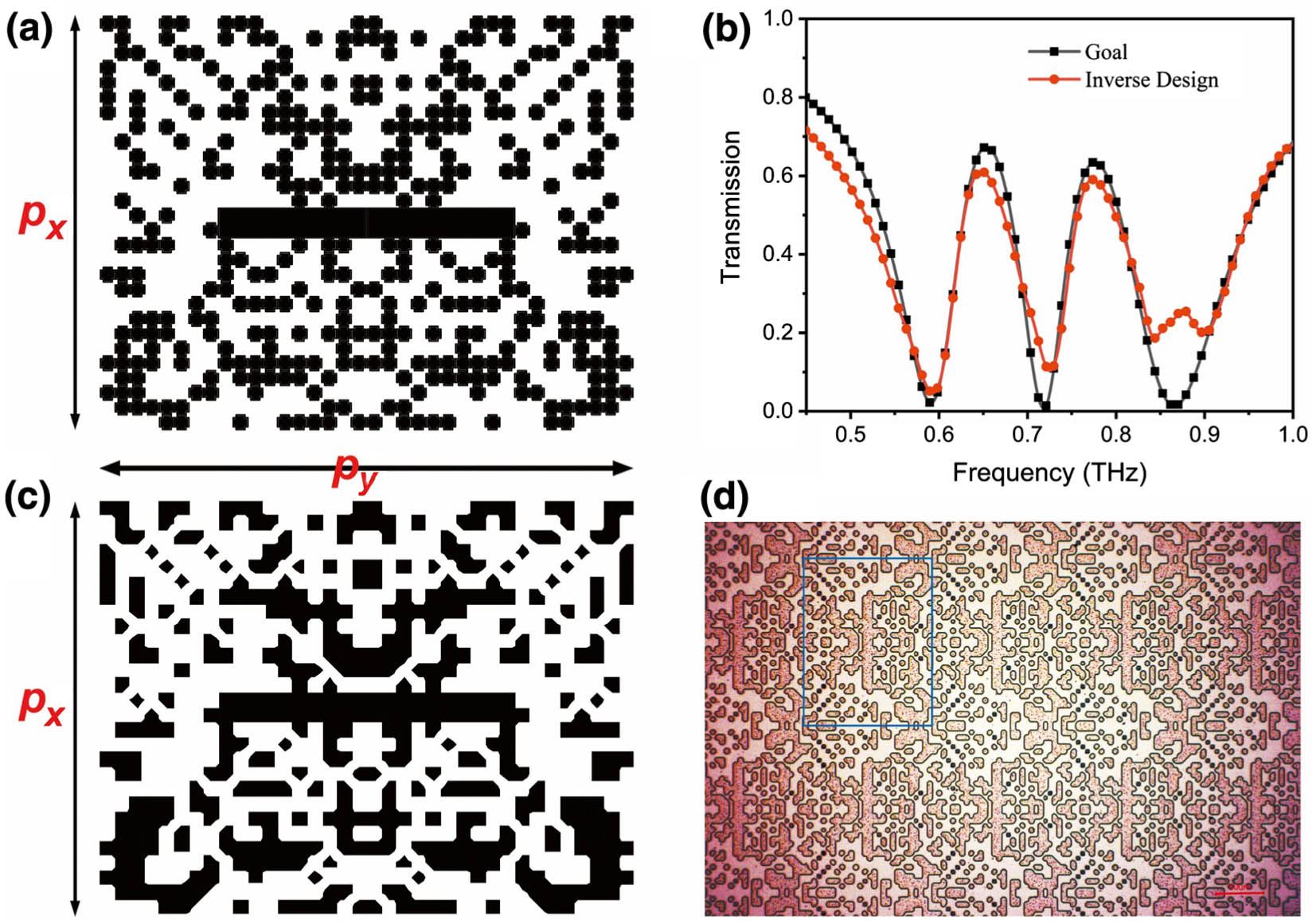
Figure 1.(a) Original inversely-designed structure, where px and py are the periods in the x and y direction, respectively. (b) The transmission spectra of the target (black) and inverse design (red). (c) Adjusted inverse design metasurface structure. (d) Processed ultimate inverse design metasurface with 200-nm-thick amorphous Ge film covering the face. The scale bar in the pictures is 50 µm.
3. Results
3.1. Active terahertz double EIT modulation
The THz transmission spectra in the finally designed metasurface are shown in Fig. 2(a); the simulation and experiment results match well, and both describe two EIT-like windows at 0.68 THz (peak1) and 0.77 THz (peak2). In the experimental measurements, we employ a THz time-domain system (TDS) to obtain the time-domain spectrum, and the frequency-domain spectrum is obtained by Fourier transform. A Ti:sapphire regenerative amplifier system is employed to generate a femtosecond pulse of 1 kHz repetition at a central wavelength of 800 nm for stimulating the ZnTe crystal for THz generation and detection as well as activating the photogenerated carrier of Ge film. The transmission spectrum is defined by
![]()
Figure 2.(a) Experimental (black) and simulated (red) transmission spectra of the ultimate inverse design metasurface. (b) Time-domain THz spectra when the THz pulse passes the quartz substrate (black) and metasurface (red). Experimental modulation of THz double EIT (c) transmission and (d) group delay for various pump fluences ranging from 0 to 2.25 mJ/cm2.
3.2. Ultrafast terahertz transmission and slow-light switching
Turning now, we discuss the dynamically tunable THz EIT-like response of the inversely-designed metasurface cooperating with amorphous Ge film. Benefiting from the ultrafast relaxation time of amorphous Ge film, the THz EIT-like modulation cycle is on the picosecond scale[
![]()
Figure 3.Experimentally extracted (a) differential transmittance and (b) transient conductivity of 200 nm pure Ge film at pump fluence of 2.25 mJ/cm2. (c), (e) Map of experimental THz transmission and group delay as a function of relative time delay between the femtosecond laser and THz pulse. (d), (f) Map of simulated THz transmission and group delay as a function of relative time delay between the femtosecond laser and THz pulse.
3.3. Near-field distributions of inversely-designed metasurface with various Ge conductivities
To reveal the physical mechanism of double EIT-like resonance and its modulation in inversely-designed metasurface combining with amorphous Ge film, the simulated near-field distributions with different Ge conductivities were monitored at 1 µm above the metasurface. In the static simulation, the conductivity of Ge film stays the same during the whole time-domain simulation (different from transient simulation). In the case of low conductivity of Ge film, i.e., 10 S/m, which was slightly tuned but still held double EIT-like resonance, the local electric field showed strong enhancement. As we can see in Figs. 4(a) and 4(c), the electric field is locally above at the frequency of peak1, and there is also a strong locality above the structure at the frequency of peak2 but more concentration below. The cut wire provides a radiation mode with weak local-field enhancement. The electric fields are localized at different positions reflecting different dark resonance modes, and double EIT-like resonances are found in the macroscopic transmission spectrum at last. Notably, it is a possibility to design multiple EIT-like resonances by adjusting the position of pixels based on the inverse design. On the other hand, in the case of high conductivity of Ge film, i.e., 1000 S/m, in which the double EIT-like resonance was completely suppressed, the intensity of the local electric field weakened, as shown in Figs. 4(b) and 4(d). Weakened electric-field intensity indicates a weakening of the THz coupling to the metasurface, which explains the THz EIT-like modulation based on light-excited semiconductors very well.
![]()
Figure 4.Static near-field simulation results. (a), (b) Near-field distributions of the inversely-designed metasurface in the first transparency window (peak1) with various conductivities of Ge film, 10 and 1000 S/m, respectively. (c), (d) Near-field distributions of the inversely-designed metasurface in the second transparency window (peak2) with various conductivities of Ge film, 10 and 1000 S/m, respectively.
4. Conclusion
In conclusion, we proposed a dual-channel THz modulator via an inversely-designed metasurface combining with Ge film. With the PSO algorithm cooperating with the FDTD method, we designed a metasurface structure with double EIT-like windows. Combined with an actively tunable semiconductor, amorphous Ge film, this metadevice enables ultrafast modulation speed of 25 ps under optical excitation. Two channels achieve 74% and 65% modulation depth, respectively. Our transient simulation results are in good agreement with the experimental test data, and near-field distributions in static simulation explain the double EIT-like modulation process. The experimental and simulated results illustrate an application of two-channel ultrafast THz encoding. Our inverse design method provides a reference for designing metadevices and points the way for high-performance THz multifunctional devices.
References
[1] L. Wang, J.-X. Sun, M.-X. Luo, Y.-H. Sun, X.-X. Wang, Y. Chen, Z.-H. Kang, H.-H. Wang, J.-H. Wu, J.-Y. Gao. Image routing via atomic spin coherence. Sci. Rep., 5, 18179(2015).
[2] L. Chen, Z. Xu, W. Zeng, Y. Wen, S. Li, H. Wang. Controllably releasing long-lived quantum memory for photonic polarization qubit into multiple spatially-separate photonic channels. Sci. Rep., 6, 33959(2016).
[3] L. Fan, K. Y. Fong, M. Poot, H. X. Tang. Cascaded optical transparency in multimode-cavity optomechanical systems. Nat. Commun., 6, 5850(2015).
[4] X. Yang, B. Xue, J. Zhang, S. Zhu. A universal quantum information processor for scalable quantum communication and networks. Sci. Rep., 4, 6629(2014).
[5] Y.-L. Chuang, R.-K. Lee, A. Y. Ite. Generation of quantum entanglement based on electromagnetically induced transparency media. Opt. Express, 29, 3928(2021).
[6] X. He, X. Yang, G. Lu, W. Yang, F. Wu, Z. Yu, J. Jiang. Implementation of selective controlling electromagnetically induced transparency in terahertz graphene metamaterial. Carbon, 123, 668(2017).
[7] Y. Hu, T. Jiang, J. Zhou, H. Hao, H. Sun, H. Ouyang, M. Tong, Y. Tang, H. Li, J. You. Ultrafast terahertz transmission/group delay switching in photoactive WSe2-functionalized metaphotonic devices. Nano Energy, 68, 104280(2020).
[8] Y. Zhao, Q. Huang, H. Cai, X. Lin, H. He, H. Cheng, T. Ma, Y. Lu. Ultrafast control of slow light in THz electromagnetically induced transparency metasurfaces. Chin. Opt. Lett., 19, 073602(2021).
[9] T. Ma, Q. Huang, H. He, Y. Zhao, X. Lin, Y. Lu. All-dielectric metamaterial analogue of electromagnetically induced transparency and its sensing application in terahertz range. Opt. Express, 27, 16624(2019).
[10] L. Zhu, H. Li, L. Dong, W. Zhou, M. Rong, X. Zhang, J. Guo. Dual-band electromagnetically induced transparency (EIT) terahertz metamaterial sensor. Opt. Mater. Express, 11, 2109(2021).
[11] C. Liu, P. Liu, C. Yang, Y. Lin, S. Zha. Dynamic electromagnetically induced transparency based on a metal-graphene hybrid metamaterial. Opt. Mater. Express, 8, 1132(2018).
[12] Y. Hu, T. Jiang, H. Sun, M. Tong, J. You, X. Zheng, Z. Xu, X. Cheng. Ultrafast frequency shift of electromagnetically induced transparency in terahertz metaphotonic devices. Laser Photonics Rev., 14, 1900338(2020).
[13] Y. Hu, M. Tong, Z. Xu, X. Cheng, T. Jiang. Spatiotemporal terahertz metasurfaces for ultrafast all-optical switching with electric-triggered bistability. Laser Photonics Rev., 15, 2000456(2021).
[14] Y.-Y. Ji, F. Fan, M. Chen, L. Yang, S.-J. Chang. Terahertz artificial birefringence and tunable phase shifter based on dielectric metasurface with compound lattice. Opt. Express, 25, 11405(2017).
[15] K. Liu, X. Chen, M. Lian, J. Jia, Y. Su, H. Ren, S. Zhang, Y. Xu, J. Chen, Z. Tian, T. Cao. Nonvolatile reconfigurable electromagnetically induced transparency with terahertz chalcogenide metasurfaces. Laser Photonics Rev., 16, 2100393(2022).
[16] H. Yao, Z. Sun, X. Yan, M. Yang, L. Liang, G. Ma, J. Gao, T. Li, X. Song, H. Zhang, Q. Yang, X. Hu, Z. Wang, Z. Li, J. Yao. Ultrasensitive, light-induced reversible multidimensional biosensing using THz metasurfaces hybridized with patterned graphene and perovskite. Nanophotonics, 11, 1219(2022).
[17] T. Zhou, S. Chen, X. Zhang, X. Zhang, H. Hu, Y. Wang. Electromagnetically induced transparency based on a carbon nanotube film terahertz metasurface. Opt. Express, 30, 15436(2022).
[18] R. Yang, Q. Fu, Y. Fan, W. Cai, K. Qiu, W. Zhang, F. Zhang. Active control of EIT-like response in a symmetry-broken metasurface with orthogonal electric dipolar resonators. Photonics Res., 7, 955(2019).
[19] Y. Hu, M. Tong, Z. Xu, X. Cheng, T. Jiang. Bifunctional spatiotemporal metasurfaces for incident angle-tunable and ultrafast optically switchable electromagnetically induced transparency. Small, 17, 2006489(2021).
[20] Z. Bai, Q. Zhang, G. Huang. Nonlinear polaritons in metamaterials with plasmon-induced transparency. Chin. Opt. Lett., 17, 012501(2019).
[21] J. Hwang, Y. Kim, Y. Yoo, K. Kim, J. Rhee, L. Chen, S. Li, X. Guo, Y. Lee. Tunable quad-band transmission response, based on single-layer metamaterials. Opt. Express, 26, 31607(2018).
[22] K. Zhang, C. Wang, L. Qin, R.-W. Peng, D.-H. Xu, X. Xiong, M. Wang. Dual-mode electromagnetically induced transparency and slow light in a terahertz metamaterial. Opt. Lett., 39, 3539(2014).
[23] S. Hu, H. Yang, S. Han, X. Huang, B. Xiao. Tailoring dual-band electromagnetically induced transparency in planar metamaterials. J. Appl. Phys., 117, 043107(2015).
[24] S. Molesky, Z. Lin, A. Y. Piggott, W. Jin, J. Vucković, A. W. Rodriguez. Inverse design in nanophotonics. Nat. Photonics, 12, 659(2018).
[25] S. So, T. Badloe, J. Noh, J. Rho, J. Bravo-Abad. Deep learning enabled inverse design in nanophotonics. Nanophotonics, 9, 1041(2020).
[26] D. Rafique, L. Velasco. Machine learning for network automation: overview, architecture, and applications [Invited Tutorial]. J. Opt. Commun. Netw., 10, D126(2018).
[27] S. D. Campbell, D. Sell, R. P. Jenkins, E. B. Whiting, J. A. Fan, D. H. Werner. Review of numerical optimization techniques for meta-device design. Opt. Mater. Express, 9, 1842(2019).
[28] B. Shen, P. Wang, R. Polson, R. Menon. An integrated-nanophotonics polarization beamsplitter with 2.4 × 2.4 µm2 footprint. Nat. Photonics, 9, 378(2015).
[29] C. M. Lalau-Keraly, S. Bhargava, O. D. Miller, E. Yablonovitch. Adjoint shape optimization applied to electromagnetic design. Opt. Express, 21, 21693(2013).
[30] M. D. Huntington, L. J. Lauhon, T. W. Odom. Subwavelength lattice optics by evolutionary design. Nano Lett., 14, 7195(2014).
[31] P. R. Wiecha, C. Majorel, C. Girard, A. Cuche, V. Paillard, O. L. Muskens, A. Arbouet. Design of plasmonic directional antennas via evolutionary optimization. Opt. Express, 27, 29069(2019).
[32] Z. Yu, H. Cui, X. Sun. Genetic-algorithm-optimized wideband on-chip polarization rotator with an ultrasmall footprint. Opt. Lett., 42, 3093(2017).
[33] Z. Lin, X. Liang, M. Lončar, S. G. Johnson, A. W. Rodriguez. Cavity-enhanced second-harmonic generation via nonlinear-overlap optimization. Optica, 3, 233(2016).
[34] Y. Yan, P. Liu, X. Zhang, Y. Luo. Photonic crystal topological design for polarized and polarization-independent band gaps by gradient-free topology optimization. Opt. Express, 29, 24861(2021).
[35] Z. Lin, V. Liu, R. Pestourie, S. G. Johnson. Topology optimization of freeform large-area metasurfaces. Opt. Express, 27, 15765(2019).
[36] B. Shen, P. Wang, R. Polson, R. Menon. Ultra-high-efficiency metamaterial polarizer. Optica, 1, 356(2014).
[37] X. Ju, G. Zhu, F. Huang, Z. Dai, Y. Chen, C. Guo, L. Deng, X. Wang. Reverse design of pixel-type terahertz band-pass filters. Opt. Express, 30, 957(2022).
[38] Y. Zhang, S. Yang, A. Eu-Jin Lim, G.-Q. Lo, C. Galland, T. Baehr-Jones, M. Hochberg. A compact and low loss Y-junction for submicron silicon waveguide. Opt. Express, 21, 1310(2013).
[39] J. C. Mak, C. Sideris, J. Jeong, A. Hajimiri, J. K. Poon. Binary particle swarm optimized 2 x 2 power splitters in a standard foundry silicon photonic platform. Opt. Lett., 41, 3868(2016).
[40] J. Li, L. Bao, S. Jiang, Q. Guo, D. Xu, B. Xiong, G. Zhang, F. Yi. Inverse design of multifunctional plasmonic metamaterial absorbers for infrared polarimetric imaging. Opt. Express, 27, 8375(2019).
[41] R. Hassan, B. Cohanim, O. de Weck, G. Venter. A comparison of particle swarm optimization and the genetic algorithm. 46th AIAA/ASME/ASCE/AHS/ASC Structures, Structural Dynamics and Materials Conference, Structures, Structural Dynamics, and Materials and Co-located Conferences(2005).
[42] W. He, M. Tong, Z. Xu, Y. Hu, X. Cheng, T. Jiang. Ultrafast all-optical terahertz modulation based on an inverse-designed metasurface. Photonics Res., 9, 1099(2021).
[43] W. Huang, J. Lin, M. Qiu, T. Liu, Q. He, S. Xiao, L. Zhou. A complete phase diagram for dark-bright coupled plasmonic systems: applicability of Fano’s formula. Nanophotonics, 9, 3251(2020).
[44] W. X. Lim, M. Manjappa, Y. K. Srivastava, L. Cong, A. Kumar, K. F. MacDonald, R. Singh. Ultrafast all-optical switching of germanium-based flexible metaphotonic devices. Adv. Mater., 30, 1705331(2018).
[45] Y. Hu, H. Hao, J. Zhang, M. Tong, X. Cheng, T. Jiang. Anisotropic temporal metasurfaces for tunable ultrafast photoactive switching dynamics. Laser Photonics Rev., 15, 2100244(2021).
[46] H. J. Joyce, J. L. Boland, C. L. Davies, S. A. Baig, M. B. Johnston. A review of the electrical properties of semiconductor nanowires: insights gained from terahertz conductivity spectroscopy. Semicond. Sci. Technol., 31, 103003(2016).


Set citation alerts for the article
Please enter your email address

© Copyright 2018-2021 | Chinese Laser Press. All Rights Reserved 沪ICP备15018463号-20