• Photonics Research
  • Vol. 4, Issue 3, 00A9 (2016)
Hironaru Murakami*, Shogo Fujiwara, Iwao Kawayama, and Masayoshi Tonouchi
Author Affiliations
  • Institute of Laser Engineering, Osaka University, 2-6 Yamadaoka, Suita, Osaka 565-0871, Japan
  • show less
    DOI: 10.1364/prj.4.0000a9 Cite this Article Set citation alerts
    Hironaru Murakami, Shogo Fujiwara, Iwao Kawayama, Masayoshi Tonouchi. Study of photoexcited-carrier dynamics in GaAs photoconductive switches using dynamic terahertz emission microscopy[J]. Photonics Research, 2016, 4(3): 00A9 Copy Citation Text show less
    Schematic of the optical-system setup for DTEM. This system can also observe laser reflection images of a sample by monitoring the reflection beam of the probe laser using a photodiode.
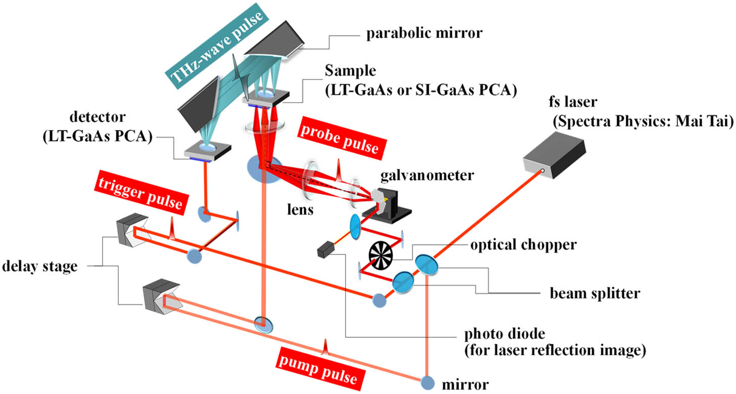
    Fig. 1. Schematic of the optical-system setup for DTEM. This system can also observe laser reflection images of a sample by monitoring the reflection beam of the probe laser using a photodiode.
    (a) Laser reflection image of LT-GaAs PCA with a 5 μm long and a 10 μm wide gap region and (b) a line profile along the inserted line in (a). The spatial resolution was estimated as ∼1.5 μm from 10% to 90% of the width of the degree of leaning of the boundary line.
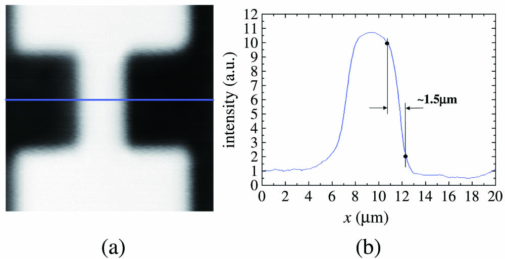
    Fig. 2. (a) Laser reflection image of LT-GaAs PCA with a 5 μm long and a 10 μm wide gap region and (b) a line profile along the inserted line in (a). The spatial resolution was estimated as 1.5  μm from 10% to 90% of the width of the degree of leaning of the boundary line.
    (a) LTEM image of the LT-GaAs PCA obtained under the laser-power conditions of Ppump=0 mW and Pprobe=1 mW and (b) DTEM image of the LT-GaAs PCA obtained before the 2.5 ps of a pump pulse irradiation under laser-power conditions of Ppump=30 mW and Pprobe=1 mW. To clarify the region of the THz pulse emission, each image is superimposed on its laser reflection image. The brightness corresponds to the strength of the THz pulse emission. (c) and (d) show the band profiles between the electrodes expected from (a) the LTEM image and (b) the DTEM image, respectively. Here, (c) indicates that the electric-field screening slightly occurs in the central gap region between the electrodes, probably due to the space charge formed between spatially separated electrons in the conduction band and the holes trapped at some localized impurity (or defect) states with a long relaxation time.
    Fig. 3. (a) LTEM image of the LT-GaAs PCA obtained under the laser-power conditions of Ppump=0  mW and Pprobe=1  mW and (b) DTEM image of the LT-GaAs PCA obtained before the 2.5 ps of a pump pulse irradiation under laser-power conditions of Ppump=30  mW and Pprobe=1  mW. To clarify the region of the THz pulse emission, each image is superimposed on its laser reflection image. The brightness corresponds to the strength of the THz pulse emission. (c) and (d) show the band profiles between the electrodes expected from (a) the LTEM image and (b) the DTEM image, respectively. Here, (c) indicates that the electric-field screening slightly occurs in the central gap region between the electrodes, probably due to the space charge formed between spatially separated electrons in the conduction band and the holes trapped at some localized impurity (or defect) states with a long relaxation time.
    Optical pump-and-probe THz emission spectra observed near the positive electrode (red), near the negative electrode (blue), and at the center (black) of the gap region, as indicated by the correspondingly colored circles in Fig. 3(b). The arrow at t=2.5 ps indicates the simultaneous irradiation of the sample with pump and probe pulses.
    Fig. 4. Optical pump-and-probe THz emission spectra observed near the positive electrode (red), near the negative electrode (blue), and at the center (black) of the gap region, as indicated by the correspondingly colored circles in Fig. 3(b). The arrow at t=2.5  ps indicates the simultaneous irradiation of the sample with pump and probe pulses.
    Time variation of a 3D map of the THz pulse amplitude emitted from a rectangular region of 12 μm×5 μm, including both electrodes, as shown in the bottom illustration. The pump pulse was irradiated to the entire LT-GaAs area at t=2.5 ps.
    Fig. 5. Time variation of a 3D map of the THz pulse amplitude emitted from a rectangular region of 12  μm×5  μm, including both electrodes, as shown in the bottom illustration. The pump pulse was irradiated to the entire LT-GaAs area at t=2.5  ps.
    Spatiotemporal 3D plot of the amplitude of the THz pulse emitted along the central line in the x direction of Fig. 3(b) [corresponding to the inserted line in Fig. 2(a)]. The red and yellow arrows indicate the middle position in the gap region between the two electrodes and the time taken for the simultaneous irradiation of the pump and probe pulses to the sample, respectively.
    Fig. 6. Spatiotemporal 3D plot of the amplitude of the THz pulse emitted along the central line in the x direction of Fig. 3(b) [corresponding to the inserted line in Fig. 2(a)]. The red and yellow arrows indicate the middle position in the gap region between the two electrodes and the time taken for the simultaneous irradiation of the pump and probe pulses to the sample, respectively.
    (a) LTEM image of the SI-GaAs PCA obtained under laser-power conditions of Ppump=0 mW and Pprobe=1 mW and (b) DTEM image of the SI-GaAs PCA obtained before the 12 ps of a pump pulse irradiation under laser-power conditions of Ppump=30 mW and Pprobe=1 mW. To clarify the region of the THz pulse emission, each image is superimposed on its laser reflection image. The brightness corresponds to the strength of the THz pulse emission. (c) and (d) show the band profiles between the electrodes expected from (a) the LTEM image and (b) the DTEM image, respectively. Here, (c) indicates that the electric-field screening strongly occurs near the positively biased electrode due to the space charge formed between spatially separated electron-hole pairs.
    Fig. 7. (a) LTEM image of the SI-GaAs PCA obtained under laser-power conditions of Ppump=0  mW and Pprobe=1  mW and (b) DTEM image of the SI-GaAs PCA obtained before the 12 ps of a pump pulse irradiation under laser-power conditions of Ppump=30  mW and Pprobe=1  mW. To clarify the region of the THz pulse emission, each image is superimposed on its laser reflection image. The brightness corresponds to the strength of the THz pulse emission. (c) and (d) show the band profiles between the electrodes expected from (a) the LTEM image and (b) the DTEM image, respectively. Here, (c) indicates that the electric-field screening strongly occurs near the positively biased electrode due to the space charge formed between spatially separated electron-hole pairs.
    DTEM image of the SI-GaAs PCA obtained before the pump pulse irradiation under the laser-power condition of Ppump=Pprobe=1 mW. To clarify the region of the THz pulse emission, the image is superimposed on its laser reflection image. In this laser-power condition, the strong screening effect due to the spatially separated electron-hole pairs was restricted, and THz pulse emission occurred more strongly near the positively biased electrode than near the negatively biased electrode.
    Fig. 8. DTEM image of the SI-GaAs PCA obtained before the pump pulse irradiation under the laser-power condition of Ppump=Pprobe=1  mW. To clarify the region of the THz pulse emission, the image is superimposed on its laser reflection image. In this laser-power condition, the strong screening effect due to the spatially separated electron-hole pairs was restricted, and THz pulse emission occurred more strongly near the positively biased electrode than near the negatively biased electrode.
    Optical pump-and-probe THz emission spectra observed near the positive electrode (red), near the negative electrode (blue), and at the center (black) of the gap region. The arrow at t=12 ps indicates the simultaneous irradiation of the pump and probe pulses to the sample.
    Fig. 9. Optical pump-and-probe THz emission spectra observed near the positive electrode (red), near the negative electrode (blue), and at the center (black) of the gap region. The arrow at t=12  ps indicates the simultaneous irradiation of the pump and probe pulses to the sample.
    Time variation of the 3D map of the THz pulse amplitude emitted from the rectangular region of 12 μm×5 μm, including both electrodes, as shown at the bottom. The pump pulse was irradiated to the entire SI-GaAs area at t=12 ps.
    Fig. 10. Time variation of the 3D map of the THz pulse amplitude emitted from the rectangular region of 12  μm×5  μm, including both electrodes, as shown at the bottom. The pump pulse was irradiated to the entire SI-GaAs area at t=12  ps.
    Spatiotemporal 3D plot of the amplitude of the THz pulse emitted along the central line in the x direction of Fig. 8(a). The red and yellow arrows indicate the middle position in the gap region between the two electrodes and the time taken for the simultaneous irradiation of the pump and probe pulses to the sample, respectively.
    Fig. 11. Spatiotemporal 3D plot of the amplitude of the THz pulse emitted along the central line in the x direction of Fig. 8(a). The red and yellow arrows indicate the middle position in the gap region between the two electrodes and the time taken for the simultaneous irradiation of the pump and probe pulses to the sample, respectively.
    Hironaru Murakami, Shogo Fujiwara, Iwao Kawayama, Masayoshi Tonouchi. Study of photoexcited-carrier dynamics in GaAs photoconductive switches using dynamic terahertz emission microscopy[J]. Photonics Research, 2016, 4(3): 00A9
    Download Citation