Abstract
We propose dynamic terahertz (THz) emission microscopy (DTEM) to visualize temporal–spatial dynamics of photoexcited carriers in electronic materials. DTEM utilizes THz pulses emitted from a sample by probe pulses irradiated after pump pulse irradiation to perform time-resolved two-dimensional mapping of the THz pulse emission, reflecting various carrier dynamics. Using this microscopy, we investigated carrier dynamics in the gap region of low-temperature-grown GaAs and semi-insulating GaAs photoconductive switches of the identical-dipole type. The observed DTEM images are well explained by the change in the electric potential distribution between the electrodes caused by the screening effect of the photoexcited electron-hole pairs.1. INTRODUCTION
The development of high-speed optoelectronic devices is necessary for obtaining advanced information in the near future. For the development of such devices, evaluation of the ultrafast dynamics of photoexcited carriers is indispensable [1–8]. Several methods using the optical pump-and-probe technique are employed for this purpose [8–17]. Among these, optical pump-and-probe terahertz (THz) emission spectroscopy (PPTS) can evaluate the dynamics of photoexcited carriers in the vicinity of the surface of electrical materials and devices [16,17]. However, PPTS can investigate the ultrafast carrier dynamics only in a local area irradiated by optical pump-and-probe pulses.
On the other hand, the laser THz emission microscope (LTEM) is a novel THz imaging tool that directly captures two-dimensional images showing the amplitude of THz pulses emitted from a sample by femtosecond optical pulse irradiation [18–20]. The LTEM can be applied to various electronic materials and devices that emit THz pulses by femtosecond optical pulse irradiation. LTEM enables the visualization of the electric-field distribution in a sample because the amplitude of the THz pulse is almost proportional to the local electric field at the femtosecond optical pulse irradiation spot. Photoexcited carriers are accelerated by the local electric field and emit a THz pulse because of the ultrafast current modulation, according to the classical formula of electrodynamics: where is the radiated electric field in the far-field approximation, and is the photoinduced current.
Another unique feature of the LTEM is its spatial resolution, which is determined by the femtosecond laser-beam spot size and not by the THz wavelength. Therefore, it is possible to obtain an LTEM image with a sub-micrometer resolution [20].
Sign up for Photonics Research TOC. Get the latest issue of Photonics Research delivered right to you!Sign up now
In the present study, we propose dynamic THz emission microscopy (DTEM), which has an unprecedented high function associating the LTEM with PPTS, and demonstrate its superior performance via the experimentally obtained spatiotemporal photoexcited-carrier dynamics in a low-temperature-grown GaAs (LT-GaAs) photoconductive antenna (PCA) and a semi-insulating GaAs (SI-GaAs) PCA.
2. EXPERIMENTAL
In the DTEM measurement, there are two ways to irradiate pump pulses to a sample. One is to irradiate the pump and probe pulses at the same position by scanning both pulses over the sample surface simultaneously. Another is to irradiate the pump pulses in a fixed area to be investigated while scanning the probe pulses over the sample surface. In the present study, the latter approach was adopted to observe the dynamics of the photoexcited carriers generated by pump pulse irradiation in the gap region of the GaAs PCA; moreover, the amplitude of a THz pulse excited by a focused probe pulse was measured and mapped as a function of the probe position by changing the time delay between the pump and probe pulses in the DTEM measurements. Therefore, the probe pulses were optically chopped for the lock-in detection of the THz pulse. In imaging, the delay stage for the probe pulses was fixed at the peak position of the time-domain waveform of the THz pulse, and the focused probe pulses were scanned over the sample surface by using a galvanometer. Thus, we observed the temporal–spatial electric-field distribution induced by photoexcited carriers through the pump pulse irradiation with a time resolution corresponding to the femtosecond pulse width.
A. Optical System Setup
Figure 1 shows a schematic of the optical system constructed for the DTEM study. A mode-locked Ti:sapphire laser (Spectra Physics; Mai Tai) produced the femtosecond optical pulses (pulse width: 100 fs; central wavelength: 800 nm; repetition rate: 82 MHz). The optical pulses were split into pump, probe, and trigger pulses by using beam splitters. The plane of polarization of the probe pulse was set perpendicular to that of the pump pulse by using a half-wave plate. The optical path of the pump pulse had a delay stage to control the optical time delay between the pump and probe pulses. An optical chopper was set in the probe path for the lock-in detection of the THz pulses excited by the probe pulses. The THz waves from the sample radiated into free space and were collimated and focused onto a detector with a dipole-type LT-GaAs PCA by using a pair of off-axis parabolic mirrors. The trigger pulses were focused onto the photoswitch region of the detector through another optical delay stage. The position of the delay stage for the trigger pulses was automatically moved using a computer for measurement of the time-domain waveform of the THz pulse and fixed at a constant position, yielding the maximum positive amplitude of the THz pulse for the measurement of DTEM images. We observed DTEM images by the scanning of the probe pulses over a square region, including the pump pulse irradiation area, on a sample surface by using a galvanometer controlled by a computer. We checked the delay time between the pump and probe pulse irradiations prior to the DTEM measurements. For this purpose, an additional optical chopper was inserted into the optical path of the pump pulse laser, and the time-domain waveforms of the THz pulses excited by the pump and probe pulses were simultaneously observed. Thus, we determined the delay time between the pulses with an accuracy of .
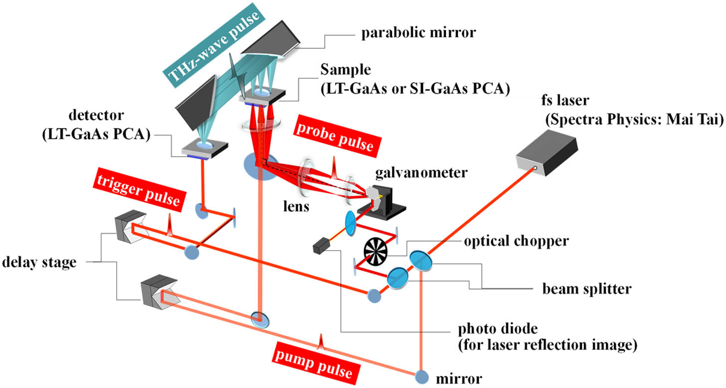
Figure 1.Schematic of the optical-system setup for DTEM. This system can also observe laser reflection images of a sample by monitoring the reflection beam of the probe laser using a photodiode.
In the measurements, we used a commercially available LT-GaAs PCA (Hamamatsu Photonics K. K.) and a homemade SI-GaAs PCA, which have an identical dipole antenna shape with 5 μm long and 10 μm wide gap regions made of Au and Au/Ti thin films, respectively. Figure 2 shows a probe laser reflection image of the LT-GaAs PCA observed by using a photodiode in this system. Here, the white and black regions correspond to LT-GaAs and Au electrodes, respectively. In the DTEM (or LTEM) measurements, the focal spot sizes of the pump and probe pulses were fixed at 12 and 1 μm, respectively. The center of the focal spot of the pump pulse was fixed at the center of the gap of PCA for the photoexcitation of the area including both electrodes.

Figure 2.(a) Laser reflection image of LT-GaAs PCA with a 5 μm long and a 10 μm wide gap region and (b) a line profile along the inserted line in (a). The spatial resolution was estimated as from 10% to 90% of the width of the degree of leaning of the boundary line.
We estimated the spatial resolution of the constructed system by using the laser reflection image. It was estimated as from 10% to 90% of the width of the degree of leaning of the boundary line in the line profile along the inserted line of Fig. 2(a). We can improve the spatial resolution to better than 0.6 μm by using an objective lens with a large numerical aperture () and a solid immersion lens with a high refractive index to reduce the focal-spot size [20].
3. RESULTS AND DISCUSSION
In the measurements, we adopted two kinds of PCAs to evaluate the performance of the constructed DTEM system. We expected to observe different characteristics between the two PCAs because of the differences in the physical properties of the photoexcited carriers, such as the mobility and lifetime. In addition to the evaluation of the system performance, it is important to investigate the dynamics of the photoexcited carriers in an LT-GaAs PCA, because LT-GaAs PCAs are conventionally used for THz pulse emitters and detectors. This study may advance our understanding of the dynamics of the electric-field screening induced by the photoexcited carriers.
Through the LTEM and DTEM measurements in the present study, we applied a direct-current bias voltage of 10 V to the electrodes of the PCA. The left and right electrodes were negatively and positively biased, respectively.
A. DTEM Studies on LT-GaAs
Prior to the investigation of the detailed dynamics of photoexcited carriers in LT-GaAs, we observed a DTEM image before the 2.5 ps of the pump pulse irradiation at a pump laser power of and a probe laser power of and observed an LTEM image without any pump pulse irradiation at and . Figures 3(a) and 3(b) show the LTEM and DTEM images, respectively, superimposed on the corresponding laser reflection images. Here, the bright region corresponds to the area where strong THz pulse emission occurred. We observe that strong THz pulse emission occurred only near the negatively biased electrode in the LTEM image without pump pulse irradiation. In addition to the THz pulse emission near the negatively biased electrode, a THz pulse emission also occurred near the positively biased electrode, as shown in the DTEM image. These results indicate that the influence of the last pump pulse remained in the DTEM measurement before the pump pulse irradiation, although there was a time interval of between the consecutive pulse irradiations. It is generally considered that the lifetime of photoexcited carriers is very short in LT-GaAs, because the photoexcited carriers are immediately captured by the stoichiometric defects caused by the excess As (As precipitates) in the material [4,5]. However, the difference between the two images apparently shows the occurrence of electric-field distortion between the two electrodes induced by the pump pulse that had been irradiated about 12 ns ago. It is considered that lots of electrons should be excited to the conduction band from the valence band, leaving positively charged holes by the pump pulse irradiation, and immediately recombine with the holes through the ultrafast scattering at As precipitates, whereas small amounts of electrons should be also excited from the As precipitates and some impurity (or defect) states lying in the mid gap region of GaAs [5,21,22]. Under these conditions small numbers of holes may be trapped at some localized impurity (or defect) states after the 12 ns of the excitation and screen the electric field in the central gap region between the electrodes by forming the weak space charge with the spatially separated electrons in the conduction band.
Figure 3.(a) LTEM image of the LT-GaAs PCA obtained under the laser-power conditions of and and (b) DTEM image of the LT-GaAs PCA obtained before the 2.5 ps of a pump pulse irradiation under laser-power conditions of and . To clarify the region of the THz pulse emission, each image is superimposed on its laser reflection image. The brightness corresponds to the strength of the THz pulse emission. (c) and (d) show the band profiles between the electrodes expected from (a) the LTEM image and (b) the DTEM image, respectively. Here, (c) indicates that the electric-field screening slightly occurs in the central gap region between the electrodes, probably due to the space charge formed between spatially separated electrons in the conduction band and the holes trapped at some localized impurity (or defect) states with a long relaxation time.
Figures 3(c) and 3(d) show the respective band profiles expected from the LTEM and DTEM images and from the above assumed conditions. It is considered that the strong THz pulse emission near the negatively biased electrode in the LTEM image was due to the large gradient of electric potential induced by the bias voltage and the band bending at the Au/GaAs interface, as shown in Fig. 3(c). On the other hand, the THz pulse emission near the positively biased electrode in the DTEM image was probably due to electric-field screening in the central region between the electrodes, as shown in Fig. 3(d).
To investigate the screening effect more carefully, PPTS measurements were performed at characteristic points inside the gap region, that is, near the positively and negatively biased electrodes and at the center between the two electrodes, as indicated by the colored circles in Fig. 3(b). Figure 4 shows the variation of the amplitude of the THz pulse excited by the probe pulse irradiation as a function of the pump-and-probe delay time. For the measurements, pump pulses irradiated the sample simultaneously with probe pulses at , as indicated by the arrow in Fig. 4. The amplitude changed abruptly after the pump pulse irradiation at . The amplitude at the center (black line) rapidly decreased, was minimized only after the pump pulse irradiation, and then almost recovered to its original state within 5 ps. In contrast, the amplitudes of the THz pulses emitted near the positively (blue line) and negatively (red line) biased electrodes rapidly increased, were maximized after the pump pulse irradiation, and then almost recovered to their original states within 4 ps. These results indicate that an electric-field screening effect occurred in the central gap region between the electrodes owing to the spatially separated electron-hole pairs excited by the pump pulse, and they also show its fast recovery—within several picoseconds—due to the very short lifetime of the photoexcited carriers in LT-GaAs [4,5].
Figure 4.Optical pump-and-probe THz emission spectra observed near the positive electrode (red), near the negative electrode (blue), and at the center (black) of the gap region, as indicated by the correspondingly colored circles in Fig. 3(b). The arrow at indicates the simultaneous irradiation of the sample with pump and probe pulses.
To obtain further detailed information about the photoexcited-carrier dynamics depending on the position in the gap region, DTEM measurements were performed by changing the delay time between the pump and probe pulses. Figure 5 shows the time variation of a three-dimensional (3D) map of the amplitude of THz pulse emissions from the rectangular region (), including both electrodes, as shown in the bottom illustration. As expected from the PPTS data shown in Fig. 4, the amplitude of the THz pulse emitted near both the Au/LT-GaAs interfaces rapidly increased and slowly recovered. The amplitude of the THz pulse along the middle of the two electrodes decreased the most and recovered because of the screening effect of the electron-hole pairs with a short lifetime of several picoseconds. Because the applied bias voltage of 10 V was constant, the screened electric field in the central region was redistributed to the areas near the positively and negatively biased electrodes. With the redistribution of the bias voltage, the amplitudes of the THz pulses emitted near both electrodes increased, whereas that of the THz pulse emitted along the middle of the two electrodes decreased, as shown in Fig. 5. In the DTEM measurements, we observed the carrier dynamics more clearly along a specific line in a sample. Figure 6 shows such a spatiotemporal 3D plot along the inserted line in Fig. 2(a). Thus, DTEM is a useful tool for evaluating the temporal–spatial dynamics of photoexcited carriers and is also excellent to detect phenomena that may be overlooked using only PPTS measurement, through the dynamic imaging.
Figure 5.Time variation of a 3D map of the THz pulse amplitude emitted from a rectangular region of , including both electrodes, as shown in the bottom illustration. The pump pulse was irradiated to the entire LT-GaAs area at .
Figure 6.Spatiotemporal 3D plot of the amplitude of the THz pulse emitted along the central line in the direction of Fig. 3(b) [corresponding to the inserted line in Fig. 2(a)]. The red and yellow arrows indicate the middle position in the gap region between the two electrodes and the time taken for the simultaneous irradiation of the pump and probe pulses to the sample, respectively.
B. DTEM Studies on SI-GaAs
The DTEM studies on SI-GaAs were conducted at approximately the same flow as those on LT-GaAs, and we first observed an LTEM image without pump pulse irradiation under laser-power conditions of and , and a DTEM image before the 12 ps of pump pulse irradiation at and . Figures 7(a) and 7(b) show the LTEM and DTEM images, respectively, superimposed on the corresponding laser reflection images. The LTEM image indicates that strong THz pulse emission occurred only near the positively biased electrode. On the other hand, the DTEM image shows that the THz pulse emission was stronger near the negatively biased electrode than near the positively biased electrode. These two images indicate that the influence of the last pump pulse strongly remained and distorted the electric-field distribution between the electrodes via the screening effect of the photoexcited carriers due to the last pump pulse in the DTEM image, as the places where the THz pulses were most strongly emitted were completely replaced between the images.
Figure 7.(a) LTEM image of the SI-GaAs PCA obtained under laser-power conditions of and and (b) DTEM image of the SI-GaAs PCA obtained before the 12 ps of a pump pulse irradiation under laser-power conditions of and . To clarify the region of the THz pulse emission, each image is superimposed on its laser reflection image. The brightness corresponds to the strength of the THz pulse emission. (c) and (d) show the band profiles between the electrodes expected from (a) the LTEM image and (b) the DTEM image, respectively. Here, (c) indicates that the electric-field screening strongly occurs near the positively biased electrode due to the space charge formed between spatially separated electron-hole pairs.
Figures 7(c) and 7(d) show the band profiles expected from the LTEM and DTEM images, respectively. Here, we first considered the electric contact conditions between SI-GaAs and Ti, as the metal electrodes made of Au/Ti used for the SI-GaAs PCA differed from those made of Au used for the LT-GaAs PCA. We deposited a Ti thin film on the SI-GaAs surface as a barrier layer to prevent the diffusion of metal atoms into SI-GaAs and to obtain a good ohmic contact with low resistance. Therefore, the band-bending condition induced in SI-GaAs near the (Au/Ti)/SI-GaAs interface should have differed from that induced in LT-GaAs near the Au/LT-GaAs interface and was considered to have the band profile illustrated in Fig. 7(c). As shown here, the band bending of SI-GaAs near the interface should have a curvature that is smaller or has the opposite sign compared with that of LT-GaAs having the interface with Au. Thus, there is a possibility that the LTEM image shows strong THz pulse emission near the positively biased electrode, which occurred because of the large electric-potential gradient induced by the bias voltage and the band bending with a curvature of opposite sign at the (Au/Ti)/SI-GaAs. Another possibility is that the electron mobility was far higher than the hole mobility in SI-GaAs [23,24] and also far higher than the electron mobility in LT-GaAs [25,26]. By adopting the mobilities of and from [23], we calculate that the photoexcited electrons could move for 1 ps, whereas the photoexcited holes could move only under an electric field of (corresponding to a bias voltage of 10 V applied to the electrodes with a gap length of 5 μm). Therefore, the photoexcited electrons near the positively biased electrodes could quickly approach the positively biased electrode and enter, while the photoexcited holes near the negatively biased electrode could not smoothly approach the opposite electrode. It is considered that these two factors—the band bending near the interface and the difference in the mobility between photoexcited electrons and holes—cooperatively acted on the strong THz pulse emission near the positively biased electrode in the LTEM image.
On the other hand, the THz pulse emission pattern observed in the DTEM measurements can be understood by considering two factors: electric-field screening by spatially separated electron-hole pairs and the difference in the mobility between the photoexcited electrons and holes.
The lifetime of the photoexcited carriers in SI-GaAs is ascribed to the consumption of the kinetic energy of the photoexcited free carriers by carrier-phonon scattering to the band edge or to form excitons and is longer than 100 ps [27]. Therefore, the negatively charged photoexcited electrons with a high mobility can move far away from the positively charged photoexcited holes under the applied bias condition and form a space charge with the spatially separated holes. Thus, it is considered that the domain of the electric-field screening due to the spatially separated electron-hole pairs is located near the positively biased electrode, as shown in Fig. 7(d). It is further considered that the THz pulse emission occurs more strongly near the negatively biased electrode than near the positively biased electrode.
As previously shown, the pump laser power of (irradiation photon density: ) is too high to investigate the dynamics of the photoexcited carriers in SI-GaAs. Therefore, we reduced until a DTEM image that was almost the same as the LTEM image in Fig. 7(a) was obtained, before the PPTS and DTEM measurements. We then conducted the following detailed DTEM studies by setting the pump laser power as (irradiation photon density: ). Figure 8 shows a DTEM image of the SI-GaAs PCA obtained before the pump pulse irradiation under the condition of . In this condition, the strong screening effect due to the spatially separated electron-hole pairs was greatly restricted, and the THz pulse emission occurred more strongly near the positively biased electrode than near the negatively biased electrode, similarly to the case of the LTEM image in Fig. 8(a).
Figure 8.DTEM image of the SI-GaAs PCA obtained before the pump pulse irradiation under the laser-power condition of . To clarify the region of the THz pulse emission, the image is superimposed on its laser reflection image. In this laser-power condition, the strong screening effect due to the spatially separated electron-hole pairs was restricted, and THz pulse emission occurred more strongly near the positively biased electrode than near the negatively biased electrode.
PPTS measurements were performed at characteristic points inside the gap region, similarly to the case of the LT-GaAs PCA. Figure 9 shows the variation of the amplitude of the THz pulse excited by the probe pulse irradiation as a parameter of the pump-and-probe delay time. For the measurements, the pump pulses irradiated the sample simultaneously with probe pulses at . The amplitude changed abruptly after the pump pulse irradiation at . The amplitude at the center (black line) rapidly decreased, was minimized after the pump pulse irradiation, and then exhibited a considerably slow recovery, but it had not recovered to its original state even after 100 ps. The amplitude of the THz pulse emitted near the positively (blue line) biased electrode also decreased. It decreased more slowly but more intensely than that in the central region (black line). It is noted that the amplitude reaches an almost zero level. In contrast, the amplitude of the THz pulse emitted near the negatively (red line) biased electrode increased after the pump pulse irradiation. The increasing curve of the blue line and the decreasing curve of the red line have shapes that contrast each other and show no sign of recovery. These results clearly suggest that the electric-field screening domain formed by the photoexcited electron-hole pairs gradually spreads out on the right side in a time scale of more than 10 ps and maintains the domain for a long time—more than 100 ps—because of the considerably long lifetime of the spatially separated electron-hole pairs.
Figure 9.Optical pump-and-probe THz emission spectra observed near the positive electrode (red), near the negative electrode (blue), and at the center (black) of the gap region. The arrow at indicates the simultaneous irradiation of the pump and probe pulses to the sample.
To obtain more detailed information about the photoexcited-carrier dynamics in SI-GaAs, DTEM measurements were performed under the laser-power condition of . Figure 10 shows the time variation of a 3D map of the amplitude of the THz pulse emission from the rectangular region () including both electrodes, as shown in the bottom illustration, and Fig. 11 shows a spatiotemporal 3D plot of the amplitude of the THz pulse emitted along the central line in the -direction of Fig. 8. As expected from the PPTS data shown in Fig. 9, the amplitudes of the THz pulses emitted near the positively and negatively biased electrodes slowly decreased and increased, respectively, and did not exhibit any recovery, even 100 ps after the pump pulse irradiation. Furthermore, the amplitude of the THz pulse emitted near the positively biased electrode almost completely disappeared at , as shown in Fig. 10. These observed photoexcited-carrier dynamics in SI-GaAs exhibit quite different characteristics from those in LT-GaAs, indicating differences in the physical and optical properties of the photoexcited carriers, such as their mobility and lifetime.
Figure 10.Time variation of the 3D map of the THz pulse amplitude emitted from the rectangular region of , including both electrodes, as shown at the bottom. The pump pulse was irradiated to the entire SI-GaAs area at .
Figure 11.Spatiotemporal 3D plot of the amplitude of the THz pulse emitted along the central line in the direction of Fig. 8(a). The red and yellow arrows indicate the middle position in the gap region between the two electrodes and the time taken for the simultaneous irradiation of the pump and probe pulses to the sample, respectively.
4. SUMMARY
We proposed DTEM to visualize the spatiotemporal dynamics of the photoexcited carriers in a variety of electronic materials and devices and constructed a basic system with a spatial resolution of and a time resolution of . We demonstrated the superior performance of the system via experiments using LT-GaAs and SI-GaAs PCAs. As for the ultrafast process of the formation of electric-field screening caused by the electron-hole pairs optically excited by pump pulse irradiation, it was revealed in LT-GaAs PCA that the screening occurred only after the pump pulse irradiation, and then almost decayed within 5 ps. On the other hand, it occurred after the pump pulse irradiation in SI-GaAs PCA, and then slowly decayed but continued even after 100 ps. Moreover, the spatiotemporal difference in the photoexcited-carrier dynamics between the PCAs, which indicates differences in the physical properties of the photoexcited free carriers such as the carrier mobility and lifetime, was demonstrated. Our results indicate that DTEM is a promising tool for evaluating the spatiotemporal dynamics of photoexcited carriers in a variety of electronic materials and devices.
References
[1] H. G. Roskos, M. C. Nuss, J. Shah, K. Leo, D. A. B. Miller, A. M. Fox, S. Schmitt-Rink, K. Kiihler. Coherent submillimeter-wave emission from charge oscillations in a double-well potential. Phys. Rev. Lett., 68, 2216-2219(1992).
[2] B. B. Hu, X.-C. Zhang, D. H. Auston. Terahertz radiation induced by subband-gap femtosecond optical excitation of GaAs. Phys. Rev. Lett., 67, 2709-2712(1991).
[3] W. Sha, J. Rhee, T. B. Norris, W. J. Schaff. Transient carrier and field dynamics in quantum-well parallel transport: from the ballistic to the quasi-equilibrium regime. IEEE J. Quantum Electron., 28, 2445-2455(1992).
[4] S. Gupta, M. Y. Frankel, J. A. Valdmanis, J. F. Whitaker, G. A. Mourou. Subpicosecond carrier lifetime in GaAs grown by molecular beam epitaxy at low temperatures. Appl. Phys. Lett., 59, 3276-3278(1991).
[5] S. Gupta, J. F. Whitaker, G. A. Mourou. Ultrafast carrier dynamics in III-V semiconductors grown by molecular-beam epitaxy at very low substrate temperatures. IEEE J. Quantum Electron., 28, 2464-2472(1992).
[6] F. W. Smith, S. Gupta, H. Q. Le, M. Frankel, V. Diadiuk, D. R. Dykaar, M. A. Hollis, G. Moumu, A. R. Calawa, T. Y. Hsiallg. Picosecond GaAs‐based photoconductive optoelectronic detectors. Appl. Phys. Lett., 54, 890-892(1989).
[7] M. Tonouchi. Cutting-edge terahertz technology. Nat. Photonics, 1, 97-105(2007).
[8] J. E. Pedersen, V. G. Lyssenko, J. M. Hvam, P. Uhd Jepsen, S. R. Keiding, C. B. Sorensen, P. E. Lindelof. Ultrafast local field dynamics in photoconductive THz antenna. Appl. Phys. Lett., 62, 1265-1267(1993).
[9] E. S. Harmon, M. R. Melloch, J. M. Woodall, D. D. Nolte, N. Otsuka, C. L. Chang. Carrier lifetime versus anneal in low temperature growth GaAs. Appl. Phys. Lett., 63, 2248-2250(1993).
[10] V. Ortiz, J. Nagle, A. Alexandrou. Influence of the hole population on the transient reflectivity signal of annealed low-temperature-grown GaAs. Appl. Phys. Lett., 80, 2505-2507(2002).
[11] R. Adomavicius, A. Krotkus, K. Bertulis, V. Sirutkaitis, R. Butkus, A. Piskarskas. Hole trapping time measurement in low-temperature-grown gallium arsenide. Appl. Phys. Lett., 83, 5304-5306(2003).
[12] A. J. Lochtefeld, M. R. Melloch, J. C. P. Chang, E. S. Harmon. The role of point defects and arsenic precipitates in carrier trapping and recombination in low‐temperature grown GaAs. Appl. Phys. Lett., 69, 1465-1467(1996).
[13] K. A. McIntosh, K. B. Nichols, S. Verghese, E. R. Brown. Investigation of ultrashort photocarrier relaxation times in low-temperature-grown GaAs. Appl. Phys. Lett., 70, 354-356(1997).
[14] H. Murakami, T. Kiwa, N. Kida, M. Tonouchi, T. Uchiyama, I. Iguchi, Z. Wang. Partial and macroscopic phase coherences in an underdoped Bi2Sr2CaCu2O8+δ thin film. Europhys. Lett., 60, 288-294(2002).
[15] M. Stellmacher, J. Nagle, J. F. Lampin, P. Santoro, J. Vaneecloo, A. Alexandrou. Dependence of the carrier lifetime on acceptor concentration in GaAs grown at low-temperature under different growth and annealing conditions. J. Appl. Phys., 88, 6026-6031(2000).
[16] M. Tonouchi, N. Kawasaki, T. Yoshimura, H. Wald, P. Seidel. Pump and probe terahertz generation study of ultrafast carrier dynamics in low-temperature-grown GaAs. Jpn. J. Appl. Phys., 41, L706-L709(2002).
[17] K. J. Siebert, A. Lisauskas, T. Löffler, H. G. Roskos. Field screening in low-temperature-grown GaAs photoconductive antennas. Jpn. J. Appl. Phys., 43, 1038-1043(2004).
[18] S. Kim, H. Murakami, M. Tonouchi. Transmission-type laser THz emission microscope using a solid immersion lens. IEEE J. Sel. Top. Quantum Electron., 14, 498-504(2008).
[19] H. Murakami, N. Uchida, R. Inoue, S. Kim, T. Kiwa, M. Tonouchi. Laser terahertz emission microscope. Proc. IEEE, 95, 1646-1657(2007).
[20] H. Murakami, K. Serita, Y. Maekawa, S. Fujiwara, E. Matsuda, S. Kim, I. Kawayama, M. Tonouchi. Scanning laser THz imaging system. J. Phys. D, 47, 374007(2014).
[21] F. Smith, A. Calawa, C.-L. Chen, M. Manfra, L. Mahoney. New MBE buffer used to eliminate backgating in GaAs MESFETs. IEEE Electron. Dev. Lett., 9, 77-80(1988).
[22] L. Landman, C. G. Morgan, J. T. Schick, P. Papoulias, A. Kumar. Arsenic interstitials and interstitial complexes in low-temperature grown GaAs. Phys. Rev. B, 55, 15581-15586(1997).
[23] J. D. Wiley, R. K. Willardson, A. C. Beer. Mobility of holes in III-V compounds. Semiconductor and Semimetals, 10, 91-174(1975).
[24] T. Matsumura, H. Emori, K. Terashima, T. Fukuda. Resistivity, Hall mobility and leakage current variations in undoped semi-insulating GaAs crystal grown by LEC method. Jpn. J. Appl. Phys., 22, L154-L156(1983).
[25] H. Nemec, A. Pashkin, P. Kuzel, M. Khazan, S. Schnull, I. Wilke. Carrier dynamics in low-temperature grown GaAs studied by terahertz emission spectroscopy. J. Appl. Phys., 90, 1303-1306(2001).
[26] C. Erginsoy. Neutral impurity scattering in semiconductors. Phys. Rev., 79, 1013-1014(1950).
[27] C. W. Siders, J. L. W. Siders, A. J. Taylor, S.-G. Park, M. R. Melloch, A. M. Weiner. Generation and characterization of terahertz pulse trains from biased, large-aperture photoconductors. Opt. Lett., 24, 241-243(1999).


