
Zheng HAN, Binfeng YUN. Design of Spectral Analysis Chip Based on Cascaded AWG[J]. Acta Photonica Sinica, 2022, 51(11): 1113003
- Acta Photonica Sinica
- Vol. 51, Issue 11, 1113003 (2022)
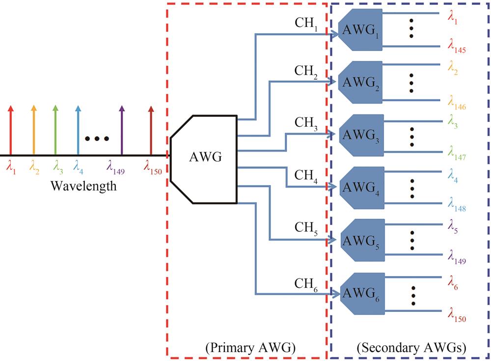
Fig. 1. Schematic diagram of the structure of the spectrum analysis chip
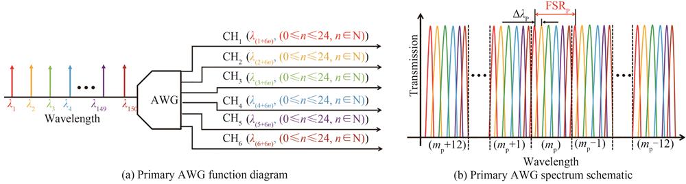
Fig. 2. Primary AWG function and spectrum schematic
Fig. 3. Schematic diagram of AWG1 function and spectrum
Fig. 4. Schematic diagram of the spectral relationship between Primary AWG CH1 and AWG1
Fig. 5. The cross-sectional view of the strip waveguide and the mode field diagram of the TE fundamental mode
Fig. 6. AWG simulation structure diagram
Fig. 7. The first-stage AWG transmission spectrum and its enlarged view in the range of 1 548.5~1 551.5 nm
Fig. 8. AWG4 transmission spectrum
Fig. 9. Spectroscopic analysis chip transmission spectroscopy
Fig. 10. The relationship between the FSRP of the Primary AWG and m
Fig. 11. Schematic diagram of the cause analysis of the large channel insertion loss and crosstalk in the edge part
|
Table 1. Design values for all AWGs
|
Table 2. Comparison between the center wavelength of the second-stage AWG obtained by simulation and the design value


Set citation alerts for the article
Please enter your email address

© Copyright 2018-2021 | Chinese Laser Press. All Rights Reserved 沪ICP备15018463号-20