• Acta Photonica Sinica
  • Vol. 51, Issue 11, 1113003 (2022)
Zheng HAN and Binfeng YUN*
Author Affiliations
  • Advanced Photonics Center,School of Electronic Science and Engineering,Southeast University,Nanjing 210096,China
  • show less
    DOI: 10.3788/gzxb20225111.1113003 Cite this Article
    Zheng HAN, Binfeng YUN. Design of Spectral Analysis Chip Based on Cascaded AWG[J]. Acta Photonica Sinica, 2022, 51(11): 1113003 Copy Citation Text show less

    Abstract

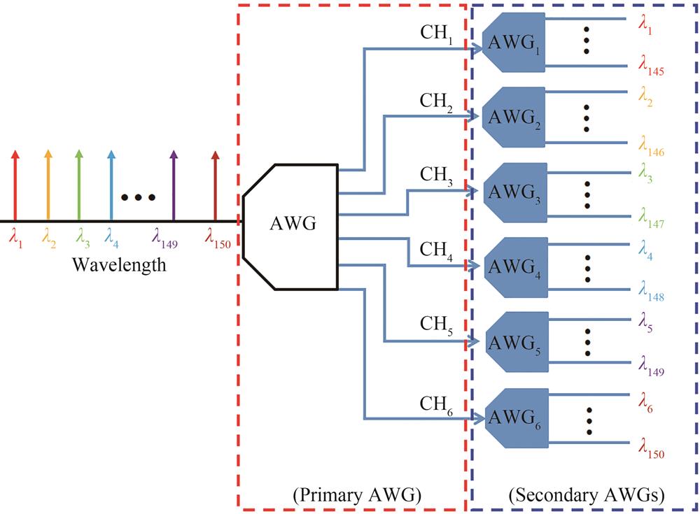
    With fast developments and wide applications of spectrum analysis, there is a great requirement for the miniaturization and chiplization of spectrum analyzer. Spectrometers based on photonic integrated chips have great advantages in size, weight and power consumption, which can be applied in many fields such as chemical and biological sensing, spectroscopy, spectral imaging and radio frequency spectrum analysis, etc. Some on-chip spectrum analyzing schemes have been proposed, such as cascading Arrayed Waveguide Grating (AWG) with Micro-Ring Resonators (MRR) and cascading multi-stage AWGs. For the scheme of cascading AWG with tunable MRRs, a long measurement time is needed due to its wavelength scanning mechanism and the crosstalk is relatively large. On the contrary, spectrum analysis chip based on cascade AWGs without wavelength scanning processes can achieve much faster spectrum acquisition.Arrayed Waveguide Grating (AWG), as a planar dispersive device, is one of the effective ways to be used as an on-chip spectrometer since it has a compact size and can be integrated with other components easily. However, it is rather difficult to achieve high resolution and large working wavelength range simultaneously with just single AWG. This intrinsic contradiction can be alleviated by cascading several AWGs. On the other hand, silicon nitride waveguide, which has the merits of low loss, transparent from visible to infrared and compatible with the Complementary Metal-Oxide-Semiconductor (CMOS) processes, has become one of the main photonic integration platforms. Various silicon nitride AWGs with low losses have been demonstrated. In this paper, a spectrum analysis chip constructed by cascading two silicon nitride AWGs is proposed, designed and optimized.In the proposed spectrum analysis chip, a silicon nitride 1×6 AWG with high resolution is cascaded with six 1×25 AWGs with coarse resolutions. By using the periodic routing property of the 1×6 AWG and setting its Free Spectral Range (FSR) equal to the channel spacing of the 1×25 AWG, spectral interleaving can be achieved between the two cascade AWG stages, then relative large working bandwidth and high resolution can be achieved simultaneously. In other words, the first stage AWG is used to provide high resolution, and the second stage AWG is used to increase the working bandwidth.In order to optimize the proposed spectrum analysis chip, the first stage AWG and the second stage AWG were designed and optimized firstly. The following results are obtained. For the primary AWG: the center wavelength, the wavelength channel spacing and the free spectral range are 1 549.90 nm, 0.5 nm and 3.0 nm, respectively. The obtained channel insertion loss, adjacent channel crosstalk and non-adjacent channel crosstalk of the center channels are about 1.2 dB, -26.1 dB and -39.0 dB, respectively. The channel insertion loss, adjacent channel crosstalk and non-adjacent channel crosstalk of edge channels are about 2.5 dB, -28.7 dB and -24.4 dB, respectively. The central wavelengths of the six secondary AWGs are set as 1 548.80 nm, 1 549.30 nm, 1 549.75 nm, 1 550.20 nm, 1 550.73 nm and 1 551.22 nm. For each secondary AWG, the wavelength channel spacing and the free spectral range are 3.0 nm and 90.0 nm, respectively. The obtained channel insertion loss, adjacent channel crosstalk and non-adjacent channel crosstalk of the center channels are about 3.6 dB, -17.8 dB and -42.2 dB, respectively. The channel insertion loss, adjacent channel crosstalk and non-adjacent channel crosstalk are about 4.5 dB, -12.7 dB and -32.3 dB, respectively. Then the obtained spectra of the cascade two-stage AWGs were multiplied to obtain the performances of the proposed spectrum analysis chip. Simulation results show that total 150 channels with wavelength resolution of 0.5 nm, which covers a working bandwidth of 75 nm can be achieved. In addition, minimum channel insertion loss of about 4.9 dB and maximum channel insertion loss of about 7.9 dB were obtained. The minimum adjacent and non-adjacent crosstalk between channels are about -27.7 dB and -23.0 dB, respectively. The maximum adjacent channel crosstalk and the maximum non-adjacent crosstalk are about -22.6 dB and -12.5 dB, respectively.According to the simulation results, we find that the performances of the middle channels are better than those of the edge channels. The reasons cause this phenomenon are analyzed theoretically and simulation results show that different FSRs are obtained for the primary AWG at different diffraction orders, while the wavelength interval of adjacent channels of the secondary AWG is the same. This will introduce center wavelength misalignment between the primary AWG and the secondary AWG, which deteriorates the insertion losses and crosstalks of the edge channels. Finally, some suggestions are given for future optimization.
    Zheng HAN, Binfeng YUN. Design of Spectral Analysis Chip Based on Cascaded AWG[J]. Acta Photonica Sinica, 2022, 51(11): 1113003
    Download Citation