Abstract
The electronic structure and optical properties of bilayer germanene under different warpages are studied by the first-principles method of density functional theory. The effects of warpages on the electronic structure and optical properties of bilayer germanene are analyzed. The results of the electronic structure study show that the bottom of the conduction band of bilayer germanene moves to the lower energy direction with the increase of warpages at the K point, and the top of the valence band stays constant at the K point, and so the band gap decreases with the increase of warpage. When the warpage is 0.075 nm, the top of the valence band of bilayer germanene changes from K point to G point, and the bilayer germanene becomes an indirect band gap semiconductor. This is an effective means to modulate the conversion of bilayer germanene between direct band gap semiconductor and indirect band gap semiconductor by adjusting the band structure of bilayer germanene effectively. The study of optical properties shows that the effect of warpage on the optical properties of bilayer germanene is mainly distributed in the ultraviolet and visible regions, and the warpage can effectively regulate the electronic structure and optical properties of bilayer germanene. When the warpage is 0.069 nm, the first peak of dielectric function and extinction coefficient is the largest, and the energy corresponding to the absorption band edge is the smallest. Therefore, the electron utilization rate is the best when the warpage is 0.069 nm.The electronic structure and optical properties of bilayer germanene under different warpages are studied by the first-principles method of density functional theory. The effects of warpages on the electronic structure and optical properties of bilayer germanene are analyzed. The results of the electronic structure study show that the bottom of the conduction band of bilayer germanene moves to the lower energy direction with the increase of warpages at the K point, and the top of the valence band stays constant at the K point, and so the band gap decreases with the increase of warpage. When the warpage is 0.075 nm, the top of the valence band of bilayer germanene changes from K point to G point, and the bilayer germanene becomes an indirect band gap semiconductor. This is an effective means to modulate the conversion of bilayer germanene between direct band gap semiconductor and indirect band gap semiconductor by adjusting the band structure of bilayer germanene effectively. The study of optical properties shows that the effect of warpage on the optical properties of bilayer germanene is mainly distributed in the ultraviolet and visible regions, and the warpage can effectively regulate the electronic structure and optical properties of bilayer germanene. When the warpage is 0.069 nm, the first peak of dielectric function and extinction coefficient is the largest, and the energy corresponding to the absorption band edge is the smallest. Therefore, the electron utilization rate is the best when the warpage is 0.069 nm.Introduction
The strange properties of graphene[1] have been studied in the field of two-dimensional materials. Graphene is a flat structure atomic layer composed of carbon atoms, a hexagonal honeycomb structure, with zero band gap of the electronic structure, high carrier mobility, and quantum spin Hall effect. Due to the semi-metallic structure of graphene with zero-band-gap, its application in electronic devices is limited to a certain extent. Germanene has well properties and can solve the problem of the limited zero band gap of graphene. The discovery of germanene opened a new world for researchers in the field of two-dimensional materials[2,3], compared to graphene, which is a folded monatomic crystal with sp2 and sp3 hybrid orbitals in the electronic structure of germanene and can easily form a folded structure. The instability of planar germanene has been confirmed by Beheraet al.[4,5]. The band structure of germanene is similar to graphene in the band structure. The valence band (VB) and the conduction band (CB) also show a linear performance energy dispersion relationship at the K point in the Brillouin region. The band gap of germanene at Dirac K point (24.3 meV) is larger than that of graphene after considering spin-orbit coupling interaction[6].
Hoshina et al. analyze the optical transition properties of Ge under six tensile strains by the first-principles calculation method. Their results showed that the direct band gap of Ge contracted faster than the indirect band gap under five tensile strains. In particular, Ge became a direct transition semiconductor under 2% tensile strain with (001) in-plane biaxial[7]. Dharet al. performed ab initio calculations of the electronic and optical properties of warpage germanene with defects (beryllium doping or void-induced). Their results showed that the Dirac cone of the germanene band structure is destroyed by doping and hole incorporation. In the semiconductor structure, the anisotropic effect is prominent in the optical properties such as dielectric function, absorption spectrum, reflectivity, modulation and conductivity[8]. Niet al. predicted that the vertical electric fields could open band gaps in semi-metallic monolayers of buckling silicon and germanene by using ab initio calculations. The size of the band gap in silicene and germanene increased linearly with the electric field intensity. Ab initio quantum transmission simulation of double gate silicon field effect transistor confirmed that the vertical electric field opened the transmission gap and also observed the significant switching effect caused by the applied gate voltage[9]. Hoatet al. proposed an effective method to artificially create germanene band gaps by chemical functionalization and doping halogen atoms. In summary, the calculation results showed that the original monolayer germanene presented semi-metallic properties at the K point using the density functional theory (DFT) method[10]. Coello-Fialloset al. studied the structure and electronic properties of bilayer graphene and bilayer germanene based on density functional theory. The results showed that bilayer graphene was an anisotropic Dirac cone. However, the π and π* bands of bilayer germanene open at the K point, forming a small band gap of 0.05 eV [11]. Qinet al. prepared bilayer germanene on the surface of Cu (111) by optimizing the preparation conditions. The calculation results showed that the bilayer germanene is formed by stacking the upper and lower layers of warped germanene (the warpage is 0.061 nm), and the bilayer germanene exhibits a perfect “V” shaped electronic state near the Fermi level[12].
In addition to bilayer germanene, researchers have carried out a lot of research on bilayer graphene. The results showed that bilayer graphene exhibits very significant band gaps and significant optical properties by different modulation modes[13-20]. Many studies have shown that different regulation modes in monolayer germanene and bilayer graphene can lead to the opening of the band gap at the Dirac point and improve the photoelectric properties of monolayer germanene[21-29] and bilayer graphene, but there are few studies on bilayer germanene. Therefore, it is important to study the electronic structure and optical properties of bilayer germanene. The electronic structure and optical properties of bilayer germanene are regulated by the degree of warping at the optimum layer spacing. The potential applications are revealed in optoelectronic industry, such as in the field of photodetectors, sensors, low-power lasers and so on. This work provides some theoretical references for the study of electronic structure and optical properties of bilayer germanene.
Calculation method and model
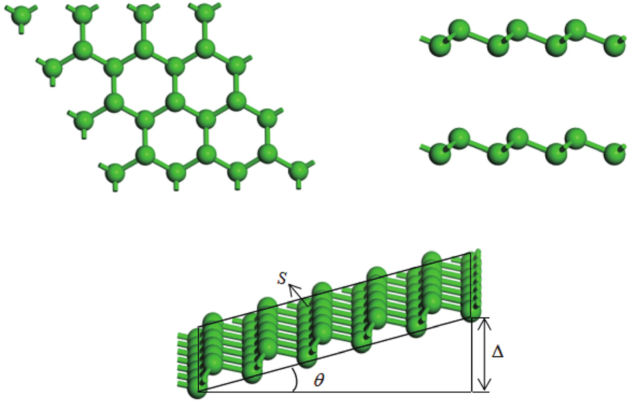
In this work, the band structure, electronic state density and optical properties of germanene are calculated by the first-principles pseudopotential plane wave method. All calculations are performed by the CASTEP (Cambridge Serial Total Energy Package) software package[30]. The generalized gradient approximation GGA(Generalized Gradient Approximation)-PW91(Perdew-Wang 91) exchange-correlation function is used to describe the exchange-correlation interaction. USPP (Ultra Soft Pseudo-Potentials) is used to process the interaction between ion cores and electrons. BFGS (Broy-den, Fletcher, Goldfarb and Shannon) method was used to optimize the geometric structure of germanene[31]. During the structural optimization, structural relaxation, energy convergence and K convergence are carried out until the force on each atom is less than 0.01 eV/Å, the self-consistent energy of the electron is less than 10–5 eV, and the pressure convergence threshold is less than 0.1 GPa. 1.5 nm vacuum layer was adopted in the Z direction to ignore external interaction. The bilayer germanene is formed by stacking the upper and lower layers of germanene with the same warping degree.Fig. 1 is a schematic diagram of the bilayer germanene structure.

Figure 1.(Color online) Schematic diagram of bilayer germanene structure.
Results and discussion
Band structure and density of states analysis
Warpage is used to describe the curvature of a plane in space. It is numerically defined as the distance between the two points farthest away from the warped plane in the direction of altitude, according to the research results of Cahangirovet al. The range of warpage is selected as 0 nm <∆ < 1 nm, and the electronic and optical properties of bilayer germanene are calculated with different warpages[3]. After optimization, the structural parameters of germanene with six different warpages are shown inTable 1, in which the lattice constant of germanene with the warpage of 0.069 nm is identical to the experimental value.
Table Infomation Is Not Enable
The band structure determines the conductivity of materials.Fig. 2 shows the band structure of bilayer germanene with different warpages. Fermi level is chosen at 0 eV and marked with dashed lines.Fig. 2(a) shows the band structure of bilayer germanene at∆1 = 0.066 nm. This figure shows that at the high symmetry K point in the Brillouin region, the top of the valence band reaches the maximum value of 0 eV at the Fermi level and the bottom of the conduction band reaches the minimum value of 0.459 eV and the forms a direct band gap semiconductor with a band gap of 0.459 eV.Fig. 2(b) shows the band structure of bilayer germanene at∆2 = 0.069 nm. This figure shows that at the high symmetry K point in the Brillouin region, the top of the valence band reaches the maximum value of 0 eV at the Fermi level and the bottom of the conduction band reaches the minimum value of 0.450 eV and forming a direct band gap semiconductor with a band gap of 0.450 eV.Figs. 2(c) and2(d) show the band structure of bilayer germanene at∆3 = 0.071 nm and∆4 = 0.073 nm, respectively. It can be seen from the figure that the direct band gap semiconductors with band gap values of 0.420 and 0.417 eV are formed at the high symmetry K point in the Brillouin region.Fig. 2(e) shows the band structure of bilayer germanene at∆5 = 0.075 nm. This figure shows that at the high symmetry point G in the Brillouin region, the top of the valence band reaches the maximum value of 0 eV at the Fermi level, and at the high symmetry K point,the bottom of the conduction band reaches the minimum value of 0.385 eV, forming an indirect band gap semiconductor with a band gap value of 0.385 eV.Fig. 2(f) shows the band structure of bilayer germanene at∆6 = 0.079 nm. This figure shows that at the high symmetry point G in the Brillouin region, the top of the valence band reaches the maximum value of 0 eV at the Fermi level, and at the high symmetric K point, the bottom of the conduction band reaches the minimum value of 0.260 eV, forming an indirect band gap semiconductor with a band gap of 0.260 eV.
Figure 2.Band structure. (a)∆1 = 0.066 nm. (b)∆2 = 0.069 nm. (c)∆3 = 0.071 nm. (d)∆4 = 0.073 nm. (e)∆5 = 0.075 nm. (f)∆6 = 0.079 nm.
It can be seen from the band structure that the size of the band gap value is mainly regulated in the conduction band, and the type of the band gap is regulated in the valence band, which has little influence on the size of the band gap. When the warpage is less than 0.075 nm, the bottom of the conduction band gradually approaches to Fermi level and remains unchanged at the K point of the Brillouin region with the increase of warpage, while the top of the valence band does not change, and there are degenerate states at the bottom of the conduction band and the top of the valence band at the K point. When the warpage is greater than 0.073 nm, the bottom of the conduction band is still close to the Fermi level at the K point, and the top of the valence band is transferred from the K point in the Brillouin region to the G point, and the bilayer germanene is transformed from a direct band gap semiconductor to an indirect band gap semiconductor. In general, with the increase of warpage, the orbital energy decreases gradually, the conduction band bottom approaches the Fermi level, and the band gap value decreases gradually. The top of the valence band shifts from the same Brillouin point to the nearest Brillouin point. The specific mechanism of change is analyzed through the density of states.
Fig. 3 shows that the warpages of bilayer germanene are∆1 = 0.066 nm,∆2 = 0.069 nm,∆3 = 0.071 nm,∆4 = 0.073 nm,∆5 = 0.075 nm,∆6 = 0.079nm. In the valence band region, the effect of warpage on bilayer germanene is mainly reflected in the energy range of –4 to 0 eV, in which the Ge 3p state electron makes the main contribution, while the Ge 3s state electron makes a small contribution. At an energy of –3.5 eV, the Ge 3p electron has a gentle peak of state density, and with the increase of warpage, the peak gradually moves to the lower energy region. At the energy of –1.5 eV, the Ge 3p state electron gradually forms an obvious peak of state density with the increase of warpage, and the total contribution of the Ge 3p state electron also gradually increases. Combined with the analysis of the band structure diagram, it is found that the change of band structure in the valence band region is mainly caused by the change of state density corresponding to these two energies.
Figure 3.(Color online) Density of states. (a)∆1 = 0.066 nm. (b)∆2 = 0.069 nm. (c)∆3 = 0.071 nm. (d)∆4 = 0.073 nm. (e)∆5 = 0.075 nm. (f)∆6 = 0.079 nm.
In the conduction band region, the effect of warpage on the bilayer germanene is mainly reflected in the energy range of 0–6 eV, and in this energy range, the main contribution is mainly made by Ge 3p electrons. At 2.8 eV, there is an obvious peak of both Ge 3p and Ge 3s electrons, which indicates the existence of sp2 and sp3 hybridization. With the increase of warpage, the hybridization of sp2 and sp3 orbital moves towards the lower energy direction. When the warpage is less than 0.075 nm, there is an obvious peak in the energy range of 2–3 eV for Ge 3p state electrons. With the increase of warpage, the peak is split into two, forming two obvious density of states peaks. In the whole energy range, the warpage has a greater effect on the electrons in the Ge 3p state than on the electrons in the Ge 3s state. The contribution of Ge 3p state electrons and Ge 3s state electrons decreases with the increase of warpage, and the distribution of Ge 3p state electrons and Ge 3s state electrons near the Fermi level changes with the change of warpage. Combined with the analysis of band structure, it can be seen that this is the main reason for the conduction band approaching the Fermi level.
Optical properties
Dielectric function
The relationship between the microphysical process of band transition and the electronic structure of solids and some spectral information can be expressed by dielectric function.Fig. 4 is the dielectric function of bilayer germanene at different warpages.Fig. 4(a) shows the real part of the dielectric function. When the warpages are∆1 = 0.066 nm,∆2 = 0.069 nm,∆3 = 0.071 nm,∆4 = 0.073 nm,∆5 = 0.075 nm,∆6 = 0.079 nm, the static dielectric constants of bilayer germanene are 20.79, 23.95, 19.35, 18.41, 17.96, 16.67, respectively. With the increase of photoelectron energy, the dielectric function of the six decreases gradually and reaches the minimum value when the photoelectron energy is 4 eV, and finally tends to a stable value. In the energy range of 0–0.15 eV, the dielectric function when the warpage is 0.069 nm obviously deviates from other dielectric functions. To explain the reasons for this, further analysis is made with the imaginary part of the dielectric function.
Figure 4.(Color online) Dielectric function. (a) Real part of the dielectric function. (b) Imaginary part of the dielectric function.
Fig. 4(b) is the imaginary part of the dielectric function of bilayer germanene at different warpages. It can be seen from the figure that the first dielectric peak of the imaginary part of the dielectric function appears in the energy range of 0–1 eV, and the first dielectric peak decreases gradually with the increase of warpage and presents a blue shift phenomenon. The results show that in bilayer germanene, the warpage is not favorable to photoelectron transition. That is, the higher the warpage is, the lower the probability of photoelectron transition is. The second dielectric peak appears around 2.8 eV, and the second dielectric peak is almost similar under different warpages, but there are slight differences in the location and size of the peak. With the increase of photoelectron energy, the dielectric peak decreases gradually, and the photoelectron transition also decreases gradually. The dielectric function changes of different warpage degrees are almost similar, which indicates that the optical properties of the bilayer germanene with low warpage have high sensitivity in the low-energy region, so it can absorb more low-energy photons. According to the density of states, the imaginary dielectric peak mainly comes from the transition from s state electron to p state electron, as the change of warpage, the electron distribution in the bilayer germanene system, the binding of surface electrons, and the nearest neighbor distance between atoms are also changed, so the dielectric function of bilayer germanene changes with the change of warpage.
Refractive index and extinction coefficient
Fig. 5(a) shows the refractive index diagram of bilayer germanene under different warpages. According to this figure, when the warpages are∆1 = 0.066 nm,∆2 = 0.069 nm,∆3 = 0.071 nm,∆4 = 0.073 nm,∆5 = 0.075 nm,∆6 = 0.079 nm, the static refractive index of bilayer germanene is 4.56, 4.89, 4.39, 4.29, 4.23, 4.08, respectively. This shows that with the increase of warpage, the interaction between bands near the Fermi level increases and the mobility of electrons decreases. Therefore, the effect of warpage on the static refractive index is similar to that of warpage on the static dielectric constant. With the increase of photoelectron energy, the refractive index of germanene decreases with different warpages, and the changing trend is the same as that of the real part of the dielectric function. In the whole energy range, the refractive index of the bilayer germanene with six different warpages is isotropic.
Figure 5.(Color online) Refractive index. (a) Refractive index. (b) Extinction coefficient.
Fig. 5(b) shows the extinction coefficient diagram. The maximum peak of the extinction coefficient appears near 0.8 eV. With the increase of the warpage, the extinction coefficient gradually decreases, indicating that the increase of the warpage is not conducive to the absorption of light. The extinction coefficient decreases with the increase of photoelectron energy. In the energy range of 3–4 eV, the extinction coefficients of bilayer germanene with∆5 = 0.075 nm and∆6 = 0.079 nm are obviously different from those of other warpages, and the extinction coefficient of bilayer germanene with different warpages shows anisotropic.
Reflectivity and absorption
Fig. 6(a) shows the reflectivity of bilayer germanene under different warpages. According to the figure, when the warpages are∆1 = 0.066 nm,∆2 = 0.069 nm,∆3 = 0.071 nm,∆4 = 0.073 nm,∆5 = 0.075 nm,∆6 = 0.079 nm, the static reflectance of bilayer germanene is 0.410, 0.436, 0.396, 0.387, 0.382, 0.368,respectively. In the energy range of 0–1 eV, the reflection characteristics decrease with the increase of warpage, indicating that the bilayer germanene with low warpage has better reflectivity in this energy range. With the increase of photoelectron energy, the reflection characteristics reach the minimum at 5 eV, and the warpage has little influence on the reflection characteristics. After that, the reflection characteristics gradually rise, reaching a maximum peak near 8.8 eV. In the energy range of 7–9 eV, the reflection characteristics decrease with the increase of warpage, indicating that warpage can significantly improve the reflectivity in this energy range. Because different warpages have different effects on the internal electron distribution and bond length in bilayer germanene, the warpage also has different effects on the reflection characteristics of bilayer germanene in different energy ranges.
Figure 6.(Color online) Reflection and absorption. (a) Reflection. (b) Absorption.
Fig. 6(b) shows the optical absorption spectrum of bilayer germanene with different warpages. It can be seen from the figure that for low-energy photons, the optical absorption changes of bilayer germanene with six different warpages are almost similar, indicating that the warpage has no obvious regulation of absorption spectrum in the low-energy region. As the photoelectron energy increases, the first small peak appears at 1 eV due to electron transitions between π and π* bands. There are three obvious absorption peaks in the vicinity of 3.8, 6.3 and 8.2 eV, respectively, indicating that photoelectron absorption is more in the vicinity of these three energies. Among them, the maximum absorption peak is in the energy range of 7–8.5 eV. In this energy range, with the increase of warpage, the intensity and width of the absorption peak gradually increase, and the maximum absorption peak moves in the direction of low energy. This shows that the warpage has a significant effect on the absorption spectrum in this energy range.
Conclusion
In this paper, the electronic structure and optical properties of bilayer germanene are calculated by the first-principles method, and the band gap and optical properties of bilayer germanene are adjusted by warpage. After geometric structure optimization, six kinds of germanene with different warpages are obtained, and the warpages are∆1 = 0.066 nm,∆2 = 0.069 nm,∆3 = 0.071 nm,∆4 = 0.073 nm,∆5 = 0.075 nm,∆6 = 0.079nm, respectively. When the warpages are∆1 = 0.066 nm,∆2 = 0.069 nm,∆3 = 0.071 nm,∆4 = 0.073 nm,∆5 = 0.075 nm,∆6 = 0.079 nm, the bilayer germanene exhibits direct band gap semiconductor withEg1 = 0.459 eV,Eg2 = 0.450 eV,Eg3 = 0.421 eV,Eg4 = 0.417 eV, respectively. When the warpages are∆5 = 0.075 nm and∆6 = 0.079 nm, the bilayer germanene exhibits an indirect band gap semiconductor withEg5 = 0.385 eV andEg6 = 0.260 eV, respectively. With the increase of warpage, the bilayer germanene is transformed from a direct bandgap semiconductor to an indirect bandgap semiconductor. Warpage can regulate the band structure and electronic density of states of bilayer germanene. The main causes of bottom conduction band shift and top valence band shift are Ge 3p state electron contribution and Ge 3P state density peak change at –1.5 eV. The effective warpage of bilayer germanene dielectric function, refractive index, reflectivity and absorption spectrum, when the warpage is less than 0.069 nm, the optical properties gradually increase with the increase of warpage; when the warpage is greater than 0.069 nm, it decreases with the increase of warpage, indicating that the optical properties are the best under the warpage of 0.069 nm, and the dielectric function, extinction coefficient, absorption band edge, and so on reach the maximum value, which effectively improves the optical utilization.
References
[1] K S Novoselov, A K Geim, S V Morozov et al. Two-dimensional gas of massless Dirac fermions in graphene. Nature, 438, 197(2005).
[2] A Kara, H Enriquez, A P Seitsonen et al. A review on silicene — New candidate for electronics. Surf Sci Rep, 67, 1(2012).
[3] S Cahangirov, M Topsakal, E Aktürk et al. Two- and one-dimensional honeycomb structures of silicon and germanium. Phys Rev Lett, 102, 236804(2009).
[4] H Behera, G Mukhopadhyay. First-principles study of structural and electronic properties of germanene. AIP Conf Proc, 1349, 823(2011).
[5] P Miro, M Audiffred, T Heine. An atlas of two-dimensional materials. Chem Soc Rev, 43, 6537(2014).
[6] T P Kaloni. Tuning the structural, electronic, and magnetic properties of germanene by the adsorption of 3d transition metal atoms. J Phys Chem C, 118, 25200(2014).
[7] Y Hoshina, K Iwasaki, A Yamada et al. First-principles analysis of indirect-to-direct band gap transition of Ge under tensile strain. Jpn J Appl Phys, 48, 04C125(2009).
[8] N Dhar, D Jana. Effect of beryllium doping and vacancy in band structure, magnetic and optical properties of free standing germanene. Curr Appl Phys, 17, 1589(2017).
[9] Z Y Ni, Q H Liu, K C Tang et al. Tunable bandgap in silicene and germanene. Nano Lett, 12, 113(2012).
[10] D M Hoat, D K Nguyen, R Ponce-Pérez et al. Opening the germanene monolayer band gap using halogen atoms: An efficient approach studied by first-principles calculations. Appl Surf Sci, 551, 149318(2021).
[11] D Coello-Fiallos, T Tene, J L Guayllas et al. DFT comparison of structural and electronic properties of graphene and germanene: Monolayer and bilayer systems. Mater Today Proc, 4, 6835(2017).
[12] Z Qin, J Pan, S Lu et al. Direct evidence of Dirac signature in bilayer germanene islands on Cu (111). Adv Mater, 29, 1606046(2017).
[13] E McCann, V I Fal'ko. Landau-level degeneracy and quantum Hall effect in a graphite bilayer. Phys Rev Lett, 96, 086805(2006).
[14] E McCann. Asymmetry gap in the electronic band structure of bilayer graphene. Phys Rev B, 74, 161403(2006).
[15] E V Castro, K S Novoselov, S V Morozov et al. Biased bilayer graphene: Semiconductor with a gap tunable by the electric field effect. Phys Rev Lett, 99, 216802(2007).
[16] J Nilsson, A H Castro Neto. Impurities in a biased graphene bilayer. Phys Rev Lett, 98, 126801(2007).
[17] M Aoki, H Amawashi. Dependence of band structures on stacking and field in layered graphene. Solid State Commun, 142, 123(2007).
[18] P Solís-Fernández, S Okada, T Sato et al. Gate-tunable Dirac point of molecular doped graphene. ACS Nano, 10, 2930(2016).
[19] N M R Peres. The electronic properties of graphene and its bilayer. Vacuum, 83, 1248(2009).
[20] J L Mañes, F Guinea, M A H Vozmediano. Existence and topological stability of Fermi points in multilayered graphene. Phys Rev B, 75, 155424(2007).
[21] H Wang, Q X Zhou, W W Ju et al. Effect of vacancy defect and dopants on the sensitivity of germanene to H 2CO. Phys E, 142, 115268(2022).
[22] M A B Hamid, K T Chan, C H Raymond Ooi et al. Structural stability and electronic properties of graphene/germanene heterobilayer. Results Phys, 28, 104545(2021).
[23] S S Raya, A S Ansari, B Shong. Adsorption of gas molecules on graphene, silicene, and germanene: A comparative first-principles study. Surf Interfaces, 24, 101054(2021).
[24] K Zhang, D Sciacca, M C Hanf et al. Structure of germanene/Al(111): A two-layer surface alloy. J Phys Chem C, 125, 24702(2021).
[25] X Si, W H She, Q Xu et al. First-principles density functional theory study of modified germanene-based electrode materials. Materials, 15, 103(2021).
[26] G Liu, W W Luo, X Wang et al. Tuning the electronic properties of germanene by molecular adsorption and under an external electric field. J Mater Chem C, 6, 5937(2018).
[27] P T Huong, D Muoi, H V Phuc et al. Low-energy bands, optical properties, and spin/valley-Hall conductivity of silicene and germanene. J Mater Sci, 55, 14848(2020).
[28] R Chegel, S Behzad. Tunable Electronic, Optical, and Thermal Properties of two-dimensional Germanene via an external electric field. Sci Rep, 10, 704(2020).
[29] V Kazemlou, A Phirouznia. Influence of compression strains on photon absorption of silicene and germanene. Superlattices Microstruct, 128, 23(2019).
[30] M D Segall, P J D Lindan, M J Probert et al. First-principles simulation: Ideas, illustrations and the CASTEP code. J Phys: Condens Matter, 14, 2717(2002).
[31] T H Fischer, A Jan. General methods for geometry and wave function optimization. J Phys Chem, 96, 9768(1992).