• Laser & Optoelectronics Progress
  • Vol. 59, Issue 19, 1922002 (2022)
Zhendong Wang, Huan Liu, Yang Chen, Yongqiang Pan, Wanpeng Xie, and Jun Han*
Author Affiliations
  • School of Armament Science and Technology, Xi'an Technological University, Xi'an 710021, Shaanxi, China
  • show less
    DOI: 10.3788/LOP202259.1922002 Cite this Article Set citation alerts
    Zhendong Wang, Huan Liu, Yang Chen, Yongqiang Pan, Wanpeng Xie, Jun Han. Design of 0.40-2.50 μm Wide-Band Optical System Based on Harmonic Diffraction Theory[J]. Laser & Optoelectronics Progress, 2022, 59(19): 1922002 Copy Citation Text show less
    Structure of the HDOE. (a) Single-layer HDOE; (b) double-layer HDOE
    Fig. 1. Structure of the HDOE. (a) Single-layer HDOE; (b) double-layer HDOE
    Bandwidth-integrated average diffraction efficiency of double-layer HDOE at different wavelengths
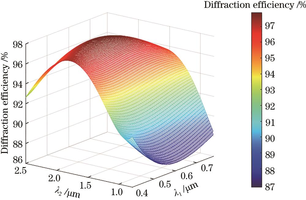
    Fig. 2. Bandwidth-integrated average diffraction efficiency of double-layer HDOE at different wavelengths
    Diffraction efficiency curve of double-layer HDOE
    Fig. 3. Diffraction efficiency curve of double-layer HDOE
    Structure of the optical system
    Fig. 4. Structure of the optical system
    MTF curve of the system. (a) 0.40-0.78 μm; (b) 0.78-2.50 μm
    Fig. 5. MTF curve of the system. (a) 0.40-0.78 μm; (b) 0.78-2.50 μm
    RMS spot diagram of the system under normal temperature conditions. (a) 0.40-0.78 μm; (b) 0.78-2.50 μm
    Fig. 6. RMS spot diagram of the system under normal temperature conditions. (a) 0.40-0.78 μm; (b) 0.78-2.50 μm
    Field curvature and distortion of the optical system. (a) 0.40-0.78 μm; (b) 0.78-2.50 μm
    Fig. 7. Field curvature and distortion of the optical system. (a) 0.40-0.78 μm; (b) 0.78-2.50 μm
    Energy diagrams of different bands. (a) 0.40-0.78 μm; (b) 0.78-2.50 μm
    Fig. 8. Energy diagrams of different bands. (a) 0.40-0.78 μm; (b) 0.78-2.50 μm
    Phase diagram of binary diffraction surface. (a) First diffraction plane; (b) second diffraction plane
    Fig. 9. Phase diagram of binary diffraction surface. (a) First diffraction plane; (b) second diffraction plane
    ParameterValue
    Wavelength /μm0.40-0.78,0.78-2.50
    Detector specifications1280×1024
    Pixel size /(μm×μm)10×10
    Focal length /mm100
    Field of view /(°)9.4×9.4
    F-number2.8
    Range of action /m1000
    Temperature range /℃-40-60
    Table 1. Design index of the optical system
    Surface tolerancesElement tolerancesIndex tolerances
    ParameterTolerancesParameterTolerancesParameterTolerances
    Fringes3Decenter(XY0.03Index0.001
    Thickness /mm0.03Tilt(XY1′Abbe /%1
    Decenter(XY0.03----
    Tilt(XY1′----
    Table 2. Tolerances of optical system
    Probability /%MTF at 50 lp/mm
    0.40-0.78 μm0.78-2.50 μm
    900.442469700.28142165
    800.476574670.30853115
    500.573651440.38551730
    200.647307620.48560952
    100.682719340.52197625
    Table 3. Analysis results of the Monte Carlo method
    Zhendong Wang, Huan Liu, Yang Chen, Yongqiang Pan, Wanpeng Xie, Jun Han. Design of 0.40-2.50 μm Wide-Band Optical System Based on Harmonic Diffraction Theory[J]. Laser & Optoelectronics Progress, 2022, 59(19): 1922002
    Download Citation