1Shandong Provincial Engineering and Technical Center of Light Manipulations & Shandong Provincial Key Laboratory of Optics and Photonic Device, School of Physics and Electronics, Shandong Normal University, Jinan 250014, China
2School of Physics and Technology, Center for Nanoscience and Nanotechnology, and Key Laboratory of Artificial Micro- and Nano-structures of Ministry of Education, Wuhan University, Wuhan 430072, China
3College of Electronics and Information Engineering, Shenzhen University, Shenzhen 518060, China
Junjun Shi, Xiaobo He, Yang Li, Hongxing Xu, "Steering of second-harmonic emission by the mode-selective excitation in a hybrid waveguide," Photonics Res. 10, 2708 (2022)
Copy Citation Text
Realization of the efficient steering for photons streams from nano sources is essential for further progress in integrated photonic circuits, especially when involving nonlinear sources. In general, steering for nonlinear sources needs additional optical control elements, limiting their application occasions as photonic devices. Here, we propose a simple and efficient beam steering scheme for the second-harmonic (SH) emission in the hybrid waveguide (consisting of CdSe nanobelts on the Au film) by mode-selective excitation. Adjusting the position of the incident beam illuminating on the tapered waveguide, the excitation types of guided modes can be selected, realizing the directionality control of SH emission. Stable steering of 6.1° for the SH emission is observed when the interference modes change from & to & , which is confirmed by SH Fourier imaging and simulations. Our approach gets rid of the complex structural design and provides a new idea for beam steering of nonlinear optical devices with various nonlinear wavefronts.
1. INTRODUCTION
Efficiently controlling and manipulating emission photons at the nanoscale level has a broad range of applications in compact optical components such as nanolasers [1,2], single photon sources [3,4], and light-emitting diodes [5,6]. Recently, extending the linear optical control to the nonlinear regime has been a novel research point. It has attracted a lot of research interest, including nonlinear volume holography [7], generation of entangled states [8], and nonlinear wavefront engineering [9]. To realize the beam steering of nonlinear sources, many approaches have been utilized, such as the phase control of effective nonlinear polarizability in nonlinear photonic metasurfaces [10–13] or by engineering the interference of multiple modes in a single particle [14–16]. However, these schemes generally require additional structural design around the nonlinear materials, which will improve the complexity of the final elements. Compared to the above nanostructures, one- or two-dimensional structures (such as nanowires or nanobelts) offer a simple and efficient manipulation degree of freedom of polarization-dependent optical response and are suitable with the waveguide system [17,18]. It is of great significance to achieve nonlinear wavefront engineering in the waveguide, which will promote the development of functionalization for nanophotonic devices [19].
Among various steering approaches, mode-selective excitation in nanostructures is considered to be a powerful means to achieve efficient and active beam steering, where the emission characters of the nano source are dependent on the type and number of the excitation modes [20,21]. To selectively excite modes into the nanostructures, different kinds of active methods are proposed such as using a spatial light modulator [21] or manipulating the phase properties of input beams [20]. Nanophotonic waveguides with high index have strong mode dispersion, which considerably minimizes intermode coupling and improves mode selectivity [22]. Directional emission has been demonstrated by selectively exciting the supported modes [17,18,23]. The excitation modes in the waveguide depend on the polarization, chirality, and phase [24,25]. The position of the excitation light will also influence the excitation modes [26]. Due to the advantage of the simple structure, easy modulation, and compatibility with the standard photonic elements, the mode-selective excitation in the waveguide will provide a feasible steering scheme for the nonlinear nano source.
Here, we demonstrate the stable beam steering of the second-harmonic generation (SHG) in a hybrid waveguide, consisting of the CdSe tapered nanobelt and the Au film. Central to our approach is the selective excitation of guided modes involved in nonlinear processes in the waveguide. We previously used a similar technique to enhance the conversion efficiency of SHG by the plasmonic grating in the waveguide [27] or modulating the types of guided modes by adjusting the diameter of the nanowires [28]. A nontrivial extension to nonlinear beam steering in one waveguide has now been realized by varying the excitation modes. In the tapered waveguide, the variety of the mode selection is outstanding and will promote the study of nonlinear beam steering. The selective excitation of different guided modes allows for influencing and directing the second-harmonic (SH) intensity distribution in the waveguide. The Fourier imaging of SHG signals confirms the interference between guided modes. The measured SH emission patterns from different excitation conditions are well in agreement with simulations. A directivity change (6.1°) for the SH emission is observed when the interference modes change from & to & at a wavelength of 800 nm. This device can potentially serve as a tunable coherent light source and promote the development of nonlinear beam engineering in integrated nanophotonics.
Sign up for Photonics Research TOC. Get the latest issue of Photonics Research delivered right to you!Sign up now
2. RESULTS AND DISCUSSION
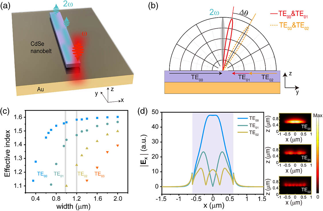
A schematic of the beam steering system based on the nanophotonic waveguide is shown in Fig. 1(a). It consists of a CdSe nanobelt and Au film, where nanobelts are synthesized by the chemical vapor deposition method [29], and the Au film (thickness 200 nm) is fabricated by the template stripping [30,31]. The CdSe nanobelt has a large nonlinear susceptibility, and the axis is along the short edge as in the transmission electron microscopy (TEM) characterization in Appendix A. The Au film acts as a mirror and promotes an efficient air coupling. The distribution of SHG in the waveguide is dependent on the excitation position of the incident light. Figure 1(a) presents the situation when the beam is focused on the corner of the edge of the waveguide. Figure 1(b) shows the far-field radiation pattern of the SHG beam at the cross-section view. The beam steering is a result of the change of participation modes in the SHG process. When the input beam is focused on the center of the edge of the tapered waveguide, the and modes are excited. When the illumination is at the corners of the tapered waveguide, the and modes are excited. Due to the momentum conservation, the wave vectors of the counterpropagating guided waves cancel each other and generate coherent SH signals along the direction perpendicular to the hybrid waveguide (gray area) [28,32,33]. This part of the SH beam is not steered when varying the excitation positions. The adjustable parts of the SH emission (orange line or red line) come from the interference between different counterpropagating modes [34,35].
Figure 1.Beam steering for SHG in a hybrid waveguide through mode-selective excitation. (a) Schematic illustration of SHG from the CdSe nanobelt placed on the top of the Au film, where the edge of the nanobelt is excited by the incident light. (b) The SHG beam steering at the cross-section view when the excitation modes change from & (red line) to & (orange line). (c) The relationship between the effective refractive index of different modes and the width. (d) Mode profiles of electric field components at z along the center of the CdSe nanobelt. The right panel shows the electric field distribution of modes , , and in the hybrid waveguide. The wavelength of excitation light is 800 nm, the width of the nanobelt is 1.2 μm, and the thickness is 120 nm.
Figure 1(c) shows the dependence of guided-mode effective refractive indices on the waveguide width W for the nanobelts of thickness 120 nm (finite element method). The wavelength of the excitation light is 800 nm. The mode refractive index increases with waveguide width growth, and the difference between the effective indices of different modes decreases with the increasing width. It is the single-mode area where only the mode is supported when the width is smaller than 0.7 μm. For widths from 0.7 to 1 μm, there are two modes ( and ) coexisting. More modes will participate in the SHG process when the width is larger than 1 μm. Figure 1(d) shows the mode profiles of the electric field components at z along the center of the CdSe nanobelt of μ. The lateral electric field component is dominant for the two even modes ( and ) and one odd mode (). These three modes can be excited with polarization parallel to the short axis of the nanobelt.
Next, we move to the experimental realization of the beam steering for SH emission in the waveguide, where the SHG measurement is performed at room temperature (more details in Appendix B). A collimated beam of a picosecond laser (NKT Photonics, EXB-4) was focused by a objective lens (, Olympus) onto the end of a CdSe nanobelt, where the diameter of the spot is 1 μm and the wavelength is 800 nm. The polarization of the incident laser was controlled by inserting a polarizer and a half-wave plate in the input optical path. We used two bandpass filters (380–420 nm) to remove the fundamental light in the SHG collection path, and the SHG signal was imported into the spectrometer (iHR 320, Horiba Jobin Yvon) for the spectroscopy or CCD camera (Retiga 3000, QImaging) for the image. A set of lenses were added to the imaging collection path to map the back focal plane of the objective. To realize the diverse excitation of modes in the waveguide, we choose a tapered nanobelt where the width is wide at the upper edge and narrow at the lower edge. Figure 2(a) shows the scanning electron microscopy (SEM) image of the hybrid waveguide where the nanobelt has a length of 13.4 μm and a width of the lower edge of 0.98 μm and the upper of 1.2 μm. The thickness of this nanobelt is . Figure 2(b) shows the SHG spectra collected from the red boxed region in Fig. 2(d), and a clear peak at 400 nm indicates the SH characteristic. The power dependence has a slope of 2.00, proving the second-order nature of the nonlinear process. The conversion efficiency of the hybrid plasmon waveguide shown in Fig. 2(d) is estimated to be , using a pump laser of 1 mW (Appendix C). The efficiency can be further improved by exciting two sides of the tapered waveguide simultaneously because SHG emission in our structures is mainly decided by the intensity of the reflected waveguide mode.
Figure 2.Nonlinear measurements with different excitation positions. (a) SEM image of a CdSe nanobelt on the Au film, with a length of 13.4 μm, and the width of the lower edge of 0.98 μm and the upper of 1.2 μm. The scale bar in panel (a) also applied in panels (d)–(e). The red arrow shows the polarization of the fundamental light. (b) Spectra of the SHG signal from the red dashed rectangular region in (d). Inset: power dependence of the SHG from the same region. A slope of 2.00 is close to the expected quadratic dependence. (c) Schematic of the supported modes with different excitation positions. (d) SHG intensity images when the excitation spot was at the center of the lower edge, like in Case (1). (e) SHG intensity images when the excitation spot was at the left corner of the upper edge, like in Case (4). (f) The setup of the Fourier imaging system and the coordinate system. (g), (h) Fourier plane images respectively from the (d) green and (e) brown box of the SHG images. The wavelength of the fundamental light is 800 nm.
According to the mode analysis with widths, there are two modes ( and ) that could be excited at the lower edge, and three modes (, , and ) are supported at the upper edge. The whole system has four cases of the mode interference. (1) When the input beam is focused on the center of the lower edge, only the mode is excited. (2) The even mode and odd mode are both excited when the input beam is moved to the right (left) corner of the lower edge. (3) At the center of the upper edge, the even modes and are both excited. (4) Three modes (, , and ) are all excited when the input light moves to the left or right corner of the upper edge. In the tapered waveguide, the mode conversion does not happen as shown in Appendix D. The excitation polarization is parallel to the short axis of the nanobelt. The Fourier image setup in Fig. 2(f) determines the direction of the SHG radiation (, ), where and are the spherical coordinates [36,37]. It enables exploration of the emission properties of the SHG photons. In Case 1, when the input beam is focused on the center of the lower edge, only the mode is excited [Figs. 2(d) and 2(g)]. The forward mode and its reflection mode will interfere with each other and generate coherent SH signals emitting in the direction perpendicular to the hybrid waveguide. This is demonstrated by the major component of the SHG emission at in the Fourier imaging. In Case 4, three modes (, , and ) are all excited when the input light moves to the left corner of the upper edge [Figs. 2(e) and 2(h)]. These modes interfere with each other and generate the periodic SHG image, and more sidelobes appear in the Fourier imaging.
We selected the interference of two modes (Case 2 and Case 3) in the experiment to achieve the nonlinear beam steering. In Case 2, when the input beam was focused on the right corner of the lower edge, even mode and odd mode are excited [Figs. 3(a) and 3(d)]. Superposition of even and odd modes results in field enhancement on one side of a single supercell and field reduction on the other side due to constructive and destructive interference of the fields [38–40]. The zigzag pattern is due to the beating of two copropagating modes ( and modes) with different propagation constants. The beating period agrees with the equation given by [28] where and are the effective refractive indices of the and mode, respectively. The counterpropagating and modes generate tilt SHG emission at , following the equation (see Appendix E) This is close to the tilt angle in the Fourier image in Fig. 3(d). In Case 3, when the incident light was focused onto the center of the upper edge of the nanobelt, and modes were excited [Figs. 3(b) and 3(e)]. The interference between and modes results in the period μ and tilt angle [Fig. 3(e)], which is also in agreement with the above equations. In Fig. 3(c), when the waveguide is illuminated on the left corner, the SHG beating pattern can be switched by half a period as compared to the SHG image in Fig. 3(a). The electric field distribution of the mode is zero on the center of the lower edge and with opposite field signs on the left and right corners as shown in Fig. 1(d). The Gaussian beam with a diameter of 1 μm only overlaps with half of the field distribution, resulting in a relative phase shift when the waveguide is exited on opposite corners. The Fourier image in Fig. 3(f) presents the same SHG emission as Fig. 3(d), further demonstrating the involved modes ( and ) in the SHG process. Beam steering of the SH emission is 6.1° when the interference modes change from & to & .
Figure 3.(a)–(c) SHG intensity images when the excitation spot was at the (a) right corner and (c) left corner of the lower edge, and (b) at the center of the upper edge. The inset shows the schematic of the excitation positions in the experiment. (d)–(f) Fourier plane images respectively from the (a) orange, (b) blue, and (c) orange box of the SHG images. The emission angles are and .
The beam steering mechanism was further confirmed by utilizing the 3D finite-difference time-domain (FDTD) simulation method (see Appendix G). We used the mode sources and selectively inputted the specific guided modes into the tapered waveguide with a length of 13.4 μm. In Fig. 4(a), we calculated the electromagnetic power density of the SHG at a plane 500 nm above the top of the waveguide. We launch the and modes at the upper edge of the tapered waveguide. The beating periodic pattern originates from the difference between effective refractive indices of the copropagating and modes, which agrees with the experiments in Fig. 3(b) and the Eq. (1). The zero momentum of SHG along the axis is from the cancelation between the same counterpropagating modes, just in the middle line of the Fourier image in Fig. 4(b). The signals deflected from the normal direction with an angle are from the interference between the input mode and the reflected , or vice versa. When the and modes are launched into the waveguide from the lower edge, the zigzag SHG pattern and Fourier imaging are reproduced as shown in Figs. 4(c) and 4(d).
Figure 4.Steering characters of SHG from the mode-selective excitation. Calculated z-component of the power flux at SH frequency when launching (a) & modes or (c) & modes into the tapered waveguide with a length of 13.4 μm. The distribution of the SH pattern relies on the types of the launched modes. The Fourier images of the SH photons with & modes in (b) and & modes in (d). The outer dashed circle of the Fourier image indicates the collection angle of the objective corresponds to 60°. (e) Measured emission angles of SHG are a function of the fundamental wavelength. represents the excitation situation of the fundamental light on the corner of the narrow edge, and represents the excitation situation of the fundamental light on the center of the wide edge of the nanobelt. The solid line is the simulated results, and the solid dots are the experiment results.
Then we studied the distribution changing of SHG emissions from the & (and & ) by varying the excitation wavelength (760–815 nm). The emission angles of SHG for both excitation conditions are a function of the excitation wavelength as shown in Fig. 4(e). The experiments agree well with the equation , and is the difference between the effective index of guided modes. We change the combination modes from & to & , and the SHG emission angles will be steered as . The steering angle of SH emission increases with the wavelength. To capture and describe further the main mechanisms that govern the SHG, we further used the dipole chain model to reproduce the experimental results very well [32] (see Appendix H). In our system, the divergence angle is , and the wavelength sensitivity was 0.06(°)/nm on average (see Appendix I). Further studies will aim at achieving the on-chip steering of SHG emissions by controlling the types of guided modes in the waveguide. Recently, utilizing the phase-gradient metasurface to manipulate the types of guided modes has been demonstrated in the waveguide [41,42], which will help realize the integrated steering nonlinear source.
3. CONCLUSION
In summary, we have demonstrated the stable and efficient beam steering of the SHG in a hybrid waveguide consisting of a CdSe nanobelt and an Au film. This was accomplished by selective excitation of three modes (, , and ) in the waveguide, and the types of excitation modes depend on the position of the incident beam on the tapered nanobelt. Our scheme uses mode-selective excitation and does not involve complex beam steering optical elements. Through Fourier imaging analysis of the SHG emission, we find that the interference between different guided mode combinations causes the SHG beam steering. We experimentally and theoretically confirmed the exact mode types involved in SHG processes, including & modes by the center excitation and & modes by the edge excitation. The beam steering angle is 6.1° when the excitation wavelength is 800 nm. This work provides new possibilities for the development of integrated nonlinear wavefront shaping photonic components.
APPENDIX A: STRUCTURAL CHARACTERIZATION FOR THE CdSe NANOBELT
We perform TEM characterization of the CdSe nanobelt (Fig. 5). The electron diffraction pattern is shown in Fig. 5(b), indicating that the axis () is perpendicular to the long axis of the nanobelt.
Figure 5.(a) TEM micrograph of a CdSe nanobelt. (b) Electron diffraction pattern of the CdSe nanobelt.
APPENDIX B: SCHEMATIC SETUP FOR THE SHG MEASUREMENT
Figure 6 shows the schematic of the SHG measurement system. A collimated beam of picosecond laser (NKT Photonics, EXB-4) was focused by a objective lens (, Olympus) onto the end of a CdSe nanobelt. The polarization of the incident laser was controlled by inserting a polarizer and a half-wave plate in the input optical path. We used two bandpass filters (FF01-400/40-25, Semrock) to remove the fundamental light in the SHG collection path, and the SHG signal was imported into the spectrometer (iHR 320, Horiba Jobin Yvon) for the spectroscopy or CCD camera (Retiga 3000, QImaging) for the image. A set of lenses were added to the imaging (EXi Blue, QImaging) collection path to map the back focal plane of the objective.
APPENDIX C: ESTIMATION OF THE SHG CONVERSION EFFICIENCY
According to our previous papers [28,33], the SHG conversion efficiency is estimated as follows. System.Xml.XmlElementSystem.Xml.XmlElementSystem.Xml.XmlElement
APPENDIX D: THE LIGHT PROPAGATION IN THE TAPERED WAVEGUIDE
As shown in Fig. 7, mode conversion does not happen in our system where these modes keep the modal characteristic.
Figure 7.Light propagation in the designed taper when the input is (a) the modal field and (b) the modal field from the left side. (c)–(e) The input is (c) the modal field, (d) the modal field, and (e) the model field from the right side.
APPENDIX E: ANALYSIS OF THE SHG PROCESS FOR COUNTERPROPAGATING MODES OF DIFFERENT TYPES
Here we considered two different kinds of oppositely propagating modes in the nanobelt, so that the fundamental electric field (ignoring the time dependence for simplicity) can be written as where , and , are the incident and reflected mode amplitudes of the two modes. The overlap will give rise to a nonlinear polarization field:
Then the nonlinear intensity is proportional to the square of the polarization field:
The SH radiated intensity varies along the waveguide as . The spatial period of this modulation is , which is in agreement with the experimental results. The term in the nonlinear polarization field induces a tilt angle in Fig. 3. Taking both momentum and energy conservation into account, we obtain the relationship between the different effective indices of the counterpropagating waves at and the SH emission angle , as or, alternatively, in terms of the effective mode indices:
Here, is the SHG wave vector, and , are the effective indices corresponding to wave vectors and .
APPENDIX F: COMPARISON EXPERIMENTS FOR PARALLEL POLARIZATION
When the excitation was along the length of the nanobelt as shown in Fig. 8, SHG signals were hardly observed in the nanobelt except for the input terminal, which is locally excited. The intensity of the SHG along the waveguide is much weaker than that along the short axis as shown in Fig. 2(d). It is because the energy of the plasmonic mode is strongly confined in the gap and suffers stronger ohmic loss than the photonic mode.
Figure 8.(a) Fault color images of SHG image, where the excitation laser at 800 nm was parallel excitation. (b) The corresponding SHG Fourier image.
APPENDIX G: CALCULATIONS OF SHG FROM A HYBRID WAVEGUIDE USING PORT INPUTS
We used 3D FDTD simulations to obtain SHG imaging and Fourier imaging through mode source input in the CdSe/Au hybrid waveguide. The width of the CdSe nanobelt is 0.98 μm or 1.20 μm, and the thickness is 120 nm. CdSe has a large refractive index according to the earlier work [43]. The permittivity of Au was taken from Johnson and Christy [44]. The CdSe nanobelts used in our experiment are wurtzite structures that belong to the 6 mm crystal class and have nonzero second-order nonlinear susceptibility components, , , and [45]. We selectively input the specific guided modes into the waveguide and obtain the electromagnetic power density at SHG frequency at a plane 500 nm above the top of the waveguide.
APPENDIX H: FOURIER IMAGES OF A CHAIN OF DIPOLES
The SHG radiated from the CdSe nanobelt is modeled as a chain of in-phase dipoles [32] () that are placed 60 nm (half of the thickness of the nanobelt) above the gold substrate as shown in Fig. 9(a). Because the electric field distributions at the fundamental and SHG frequency are polarized on the axis, the far-field calculation is performed to get the radiation patterns with the point electric dipole oscillated along the axis (TE). The chains are placed in a zigzag pattern with the same period and displacement as in the experiments. We calculated the electromagnetic power density at a plane 500 nm above the top of the waveguide as shown in Fig. 9(b). Figures 9(c) and 9(d) show the SHG Fourier imaging from the white and yellow boxed regions in the image in Fig. 9(b). The SHG radiation pattern from the chain dipole model reproduced the results from the experiments and the mode-input simulations.
Figure 9.(a) Schematic illustration of a chain of SH dipoles. (b) Electric field distribution at the cross section. (c), (d) Fourier imaging from different collection areas: (c) white and (d) orange boxes in panel (b).
Figure 10(a) shows the Fourier image when the excitation spot was at the center of the upper edge in our waveguide. In the longitudinal direction, it exhibits a narrow peak with a full width at half-maximum (FWHM) of 0.9° [Fig. 10(b)]. In Fig. 4, we confirmed a steering range of of 3° for a wavelength variation of 50 nm. The wavelength sensitivity was 0.06(°)/nm on average.
Figure 10.(a) Fourier image when the excitation spot was at the center of the upper edge in our waveguide. (b) Intensity distribution versus along the orange line in panel (a).
Junjun Shi, Xiaobo He, Yang Li, Hongxing Xu, "Steering of second-harmonic emission by the mode-selective excitation in a hybrid waveguide," Photonics Res. 10, 2708 (2022)