• Photonics Research
  • Vol. 8, Issue 2, 121 (2020)
Zhenwei Xie1、2、3、†, Ting Lei1、4、†, Haodong Qiu2, Zecen Zhang2, Hong Wang2, and Xiaocong Yuan1、*
Author Affiliations
  • 1Nanophotonics Research Center, Shenzhen Key Laboratory of Micro-scale Optical Information Technology, Institute of Microscale Optoelectronics, Shenzhen University, Shenzhen 518060, China
  • 2School of Electrical and Electronic Engineering, Nanyang Technological University, Singapore 639798, Singapore
  • 3e-mail: ayst3_1415926@sina.com
  • 4e-mail: leiting@szu.edu.cn
  • show less
    DOI: 10.1364/PRJ.8.000121 Cite this Article Set citation alerts
    Zhenwei Xie, Ting Lei, Haodong Qiu, Zecen Zhang, Hong Wang, Xiaocong Yuan. Broadband on-chip photonic spin Hall element via inverse design[J]. Photonics Research, 2020, 8(2): 121 Copy Citation Text show less
    Principles and structural design of the on-chip broadband photonic spin element. (a) Schematic of the on-chip broadband photonic spin element. The device is designed using a typical SOI configuration. The top silicon layer is 220 nm thick, the thickness of the silica layer is 2 μm, and the substrate thickness is 675 μm. The waveguide width is 440 nm. Incident light is coupled into different waveguides according to its spin states. (b) The device area is set as a black box. The phase response of the two arms is anti-symmetric for horizontal polarization and symmetric for vertical polarization. Therefore, when the incident beam is LCP (RCP), the coupled light in the left (right) arm is enhanced, and the light in the right (left) arm is cancelled out. (c) The design area is a circular area with a diameter of 2.4 μm composed of 288 pixels, each of which is a nano-arc area that can be filled either with a silicon or air block. The material distribution is optimized via inverse design. The green blocks indicate the optimized structures and are filled with silicon, while the other blocks are filled with air. (d) SEM image of the fabricated device. The scale bar is 1 μm.
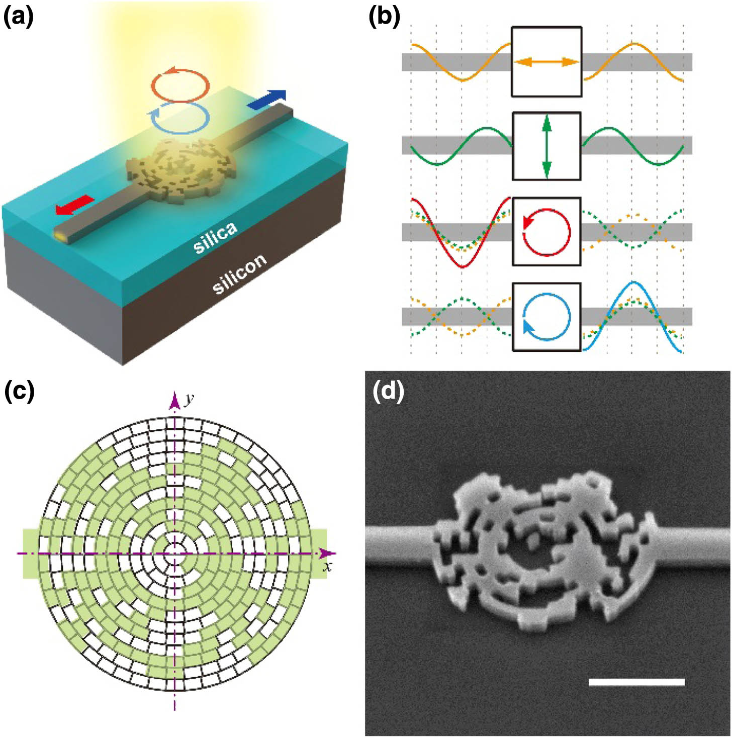
    Fig. 1. Principles and structural design of the on-chip broadband photonic spin element. (a) Schematic of the on-chip broadband photonic spin element. The device is designed using a typical SOI configuration. The top silicon layer is 220 nm thick, the thickness of the silica layer is 2 μm, and the substrate thickness is 675 μm. The waveguide width is 440 nm. Incident light is coupled into different waveguides according to its spin states. (b) The device area is set as a black box. The phase response of the two arms is anti-symmetric for horizontal polarization and symmetric for vertical polarization. Therefore, when the incident beam is LCP (RCP), the coupled light in the left (right) arm is enhanced, and the light in the right (left) arm is cancelled out. (c) The design area is a circular area with a diameter of 2.4 μm composed of 288 pixels, each of which is a nano-arc area that can be filled either with a silicon or air block. The material distribution is optimized via inverse design. The green blocks indicate the optimized structures and are filled with silicon, while the other blocks are filled with air. (d) SEM image of the fabricated device. The scale bar is 1 μm.
    Simulated electromagnetic field intensity and amplitude profiles when the device is illuminated with different polarizations. (a)–(e) Intensity profiles when the polarizations of the incident beam are LCP, RCP, 0°, 90°, and 45°, respectively. (f)–(j) Corresponding amplitude profiles.
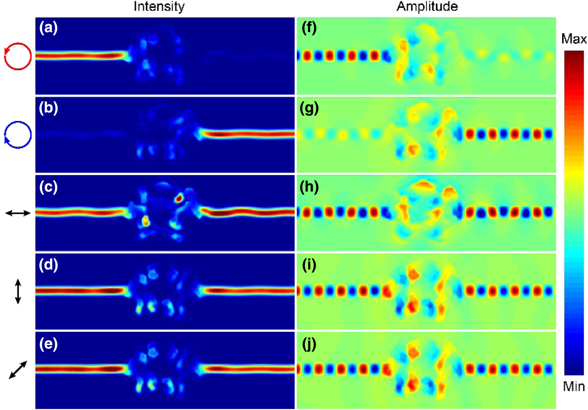
    Fig. 2. Simulated electromagnetic field intensity and amplitude profiles when the device is illuminated with different polarizations. (a)–(e) Intensity profiles when the polarizations of the incident beam are LCP, RCP, 0°, 90°, and 45°, respectively. (f)–(j) Corresponding amplitude profiles.
    Experimental measurements for using the device as an ellipsometer. (a) Experimental setup. The red arrows indicate the propagating direction of the light. PC, polarization controller; NIR, near-infrared; BS, beam splitter; CCD, charge-coupled device; QWP, quarter-wave plate; LP, linear polarizer. (b) and (c) Measured output power from the left and right arms (ports 1 and 2) of the device, respectively, when the incident beam is LCP, RCP, and LP. (d) Measured output power from the left/right arm (port 1/2) of the device when the polarization of the incident beam varies from circular to linear. (e) Comparison between measured (hollow dots) and theoretically predicted (colored solid line) ellipticities.
    Fig. 3. Experimental measurements for using the device as an ellipsometer. (a) Experimental setup. The red arrows indicate the propagating direction of the light. PC, polarization controller; NIR, near-infrared; BS, beam splitter; CCD, charge-coupled device; QWP, quarter-wave plate; LP, linear polarizer. (b) and (c) Measured output power from the left and right arms (ports 1 and 2) of the device, respectively, when the incident beam is LCP, RCP, and LP. (d) Measured output power from the left/right arm (port 1/2) of the device when the polarization of the incident beam varies from circular to linear. (e) Comparison between measured (hollow dots) and theoretically predicted (colored solid line) ellipticities.
    Broadband properties. (a) Simulated results for using the device as a photonic spin detector. The 3 dB bandwidth is over 200 nm. (b) Simulated results for using the device as a photonic spin emitter. The working bandwidth is from 1300 to 1900 nm.
    Fig. 4. Broadband properties. (a) Simulated results for using the device as a photonic spin detector. The 3 dB bandwidth is over 200 nm. (b) Simulated results for using the device as a photonic spin emitter. The working bandwidth is from 1300 to 1900 nm.
    Experimental measurements for generating circularly polarized light. (a) Experimental setup. The red arrows indicate the path flow of the light. PC, polarization controller; NIR, near-infrared; BS, beam splitter; CCD, charge-coupled device; QWP, quarter-wave plate; LP, linear polarizer. (b) Normalized measured power of the two generated circular polarizations. The lines in warm (cold) colors represent measured power when the incident light comes from the left (right) arm of the device [port 1 (port 2)] at the wavelengths 1528, 1550, 1575, and 1608 nm.
    Fig. 5. Experimental measurements for generating circularly polarized light. (a) Experimental setup. The red arrows indicate the path flow of the light. PC, polarization controller; NIR, near-infrared; BS, beam splitter; CCD, charge-coupled device; QWP, quarter-wave plate; LP, linear polarizer. (b) Normalized measured power of the two generated circular polarizations. The lines in warm (cold) colors represent measured power when the incident light comes from the left (right) arm of the device [port 1 (port 2)] at the wavelengths 1528, 1550, 1575, and 1608 nm.
    Zhenwei Xie, Ting Lei, Haodong Qiu, Zecen Zhang, Hong Wang, Xiaocong Yuan. Broadband on-chip photonic spin Hall element via inverse design[J]. Photonics Research, 2020, 8(2): 121
    Download Citation