1Nanophotonics Research Center, Shenzhen Key Laboratory of Micro-scale Optical Information Technology, Institute of Microscale Optoelectronics, Shenzhen University, Shenzhen 518060, China
2School of Electrical and Electronic Engineering, Nanyang Technological University, Singapore 639798, Singapore
The photonic spin Hall effect plays an important role in photonic information technologies, especially in on-chip spin Hall devices. However, conventional devices suffer from low efficiency or narrow bandwidth, which prevents their practical application. Here, we introduce a spin Hall device using inverse design to achieve both high efficiency and broadband. Spin-dependent light separation is enabled by a 2.4 μm circular device with 100 nm pixels. The photonic spin Hall element is fabricated on a silicon-on-insulator wafer compatible with a standard integrated photonic circuit. The spin light is detected and emitted with an efficiency of up to 22% and 35%, respectively, over a 200 nm bandwidth at optical wavelength.
1. INTRODUCTION
A photonic spin Hall (PSH) device sorts photons with different spin states and is a fundamental component of photonic information technologies [1,2]. In early work, researchers used a quarter-wave plate (QWP) and linear polarizer to distinguish photonic spins [left-circularly polarized (LCP) and right-circularly polarized (RCP)] [3]. This approach is efficient but too bulky for on-chip applications. Since the photonic spin Hall effect (PSHE) was discovered from the Imbert–Fedorov effect and optical Magnus effect [4–8], it has been considered a way to distinguish photonic spins. However, the PSHE is rather weak for measuring, and its devices are also bulky [8–10]. A metasurface is a promising way to dramatically shrink an optical element [11–14] to a size suitable for photonic spin devices. Using V-shaped nano-antennas [15], a metasurface device with a strong PSHE was demonstrated at normal incidence [16]. The emergence of a variety of Pancharatnam–Berry (PB) phase components [17–22] has led to development of various photonic spin devices, such as the directional polarization coupler [23], spin-optical metamaterial [24], broadband photonic spin resolver [25], metaspiral plasmonic lens [26], Rashba-type plasmonic metasurface [27,28], polarization-controlled surface plasmon polariton coupler [29], and conic-shaped and catenary-shaped photonic spin metasurfaces [30–32]. Researchers also demonstrated the spin Hall momentum shift and radial spin Hall effect for light using the PB phase gradient [33–35]. However, most of these devices have low efficiency. On-chip photonic spin devices that are based on spin-orbital coupling and use micro-disks and nano-antennas were reported [36,37]. The intrinsic resonance in their design limits their bandwidth and prevents their wide use. Inverse design has been successful in various situations [38,39] and has been recently introduced to photonic devices, including the ultracompact on-chip beam splitter [40] and wavelength demultiplexer [41,42].
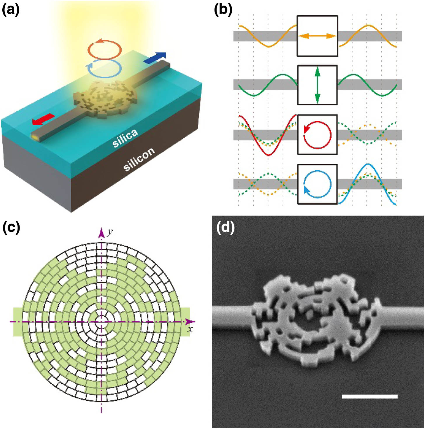
Here, we propose and demonstrate a broadband on-chip photonic spin Hall device using inverse design. As shown in Fig. 1(a), the device is designed for a standard silicon-on-insulator (SOI) wafer, and it can couple light into its left- or right-arm waveguides, according to the spin states of the incident beams. The top silicon layer is 220 nm thick, the thickness of the silica layer is 2 μm, and the substrate thickness is 675 μm. The waveguide width is 440 nm. Figure 1(b) illustrates the principle of the proposed device. The device area is set as a black box with different phase responses depending on the polarization of the incident beam. When incident light is horizontally polarized, the phases of the coupled light in the two arms are anti-symmetric, so the phase responses of the arms are opposite. In contrast, when incident light is vertically polarized, the phases of the coupled light in the two arms are symmetric, so their phase responses are the same. Therefore, the LCP light is coupled to the left arm and cancelled in the right arm. Similarly, the RCP light is coupled to the right arm and cancelled in the left. Although similar phase responses can be realized with spin-orbital coupling [36,37], the working bandwidth of the devices is usually limited by the intrinsic resonance.
Figure 1.Principles and structural design of the on-chip broadband photonic spin element. (a) Schematic of the on-chip broadband photonic spin element. The device is designed using a typical SOI configuration. The top silicon layer is 220 nm thick, the thickness of the silica layer is 2 μm, and the substrate thickness is 675 μm. The waveguide width is 440 nm. Incident light is coupled into different waveguides according to its spin states. (b) The device area is set as a black box. The phase response of the two arms is anti-symmetric for horizontal polarization and symmetric for vertical polarization. Therefore, when the incident beam is LCP (RCP), the coupled light in the left (right) arm is enhanced, and the light in the right (left) arm is cancelled out. (c) The design area is a circular area with a diameter of 2.4 μm composed of 288 pixels, each of which is a nano-arc area that can be filled either with a silicon or air block. The material distribution is optimized via inverse design. The green blocks indicate the optimized structures and are filled with silicon, while the other blocks are filled with air. (d) SEM image of the fabricated device. The scale bar is 1 μm.
Thus, we implement inverse design using a joint path and resonance phase modulation to reduce the structural size and further expand the bandwidth. This achieves a broadband device. As shown in Fig. 1(c), the device area is a circle with a diameter of 2.4 μm divided into 288 nano-arc-shaped pixels, typically smaller than 100 nm. Each pixel can be filled with either a silicon or air block. The material distribution is optimized with an inverse design to achieve the desired functionality. Our global optimization combines the annealing algorithm and the genetic algorithm associated with three-dimensional finite-difference time domain (FDTD) simulations [41,43]. A random mixture of several best guesses is used to construct a new guess that expands the search space without adding too much computational load. The figure of merit (FOM) of the optimization is defined as the average coupling efficiency in the two arms for the two circular polarizations. The initial annealing temperature is set as the maximum difference between the coupling efficiency of the two circular polarizations, to ensure a large search space, while avoiding extra computational load.
Sign up for Photonics Research TOC. Get the latest issue of Photonics Research delivered right to you!Sign up now
The optimization procedure is as follows. (1) Because there are only two possible states (air or silicon) for each pixel, the initial guess is set as a random mixture of the two materials for convenience. Then the coupling efficiencies are recorded for both circular polarizations through an FDTD simulation. The initial FOM is also calculated. (2) After randomly choosing a pixel and flipping its state (from air to silicon or vice-versa), we run the FDTD simulations to get another FOM. If the FOM is improved, its new value is recorded, the pixel flip operation is accepted, and the material distribution is set as the best so far (BSF). If the FOM becomes worse, its new value and the flip operation are accepted with a probability of , where is the average coupling efficiency of both circular polarizations in the -th iteration, and is their efficiency in the last iteration. In this condition, if the FOM and flip are accepted, then the material distribution is restored as the second best so far (SBSF). The new guess for the next iteration is obtained by randomly mixing the BSF and SBSF. (3) When all the pixels are flipped, the annealing temperature is then reduced according to , where 0.98 is defined as the cooling rate. (4) The iterations continue until the FOM reaches its maximum or the process exceeds the maximum number of iterations. Although the simulated annealing does not guarantee a global optimization, we can increase the possibility by adjusting the initial temperature, the cooling rate, and the formation of the new guess.
The annealing program is running on a workstation. The processor of the workstation is Intel Xeon Processor E7-8870 v4, it contains 20 cores and 40 threads, and each core has a base frequency of 2.3 GHz. The total memory of the workstation is 1 TB. The operating system is Windows Server 2012 R2, edition. The average annealing time is around 150 h. After the optimization, we get the final material distribution of the device area. Figure 1(d) is the SEM image of the fabricated device with a scale bar of 1 μm. The optimized device does not have a regular shape such as a square, triangle, or circle, but a more random pattern.
To investigate the functionality of the device, we implement an FDTD simulation under illumination with both circular polarization states (LCP and RCP) and with the linearly polarized (LP) states of 0°, 90°, and 45°. The simulation results in Fig. 2 show that the light couples into the left arm when the incident beam is LCP and into the right arm when the incident beam is RCP. The light couples equally into both arms when the incident beam is LP (0°, 90°, or 45°).
Figure 2.Simulated electromagnetic field intensity and amplitude profiles when the device is illuminated with different polarizations. (a)–(e) Intensity profiles when the polarizations of the incident beam are LCP, RCP, 0°, 90°, and 45°, respectively. (f)–(j) Corresponding amplitude profiles.
We experimentally demonstrated the ability of the device to measure the elliptical polarization states of the incident light beam. Figure 3(a) shows the experimental setup with a tunable near-infrared laser as the light source. A linear polarizer was used to initialize the polarization of the incident beam. A QWP was used to change linear into circular or elliptical polarization according to its orientation angle . The initial angle of the QWP was 45° relative to the linear polarizer. Therefore, the generated light was RCP when . The device was characterized with a microscopic system. The coupled light in the two arms was collected with lensed fibers and measured with power meters. First, the QWP orientation angles were set as 45°, 90°, and 180° to measure the LP, LCP, and RCP light, respectively, at wavelengths from 1528 to 1608 nm. Figures 3(b) and 3(c) show the measured output powers from the left (port 1) and right (port 2) arms, respectively. When the incident beam is LCP, the measured output power mainly comes from port 1 of the device (red dots linked with the red solid line). When the incident beam is RCP, the measured output power mainly comes from port 2 (blue dots linked with the blue solid line). When the incident beam is LP, the output powers from ports 1 and 2 are equal (black dots linked with the black solid line). The measured extinction ratios between the two circular polarizations are higher than 20 dB in the wavelength range from 1528 to 1608 nm. The extinction ratio is defined as for port 1 and for port 2. This verifies that the proposed device is a broadband on-chip photonic spin sorter.
Figure 3.Experimental measurements for using the device as an ellipsometer. (a) Experimental setup. The red arrows indicate the propagating direction of the light. PC, polarization controller; NIR, near-infrared; BS, beam splitter; CCD, charge-coupled device; QWP, quarter-wave plate; LP, linear polarizer. (b) and (c) Measured output power from the left and right arms (ports 1 and 2) of the device, respectively, when the incident beam is LCP, RCP, and LP. (d) Measured output power from the left/right arm (port 1/2) of the device when the polarization of the incident beam varies from circular to linear. (e) Comparison between measured (hollow dots) and theoretically predicted (colored solid line) ellipticities.
The QWP was then rotated from 0° to 360° to generate a varying elliptical polarization and further investigate the device performance. In Fig. 3(d), the red dots linked with the solid red line represent the measured output power from the left arm (port 1) of the device, and the blue dots linked with the solid blue line show the measured output power from the right arm (port 2). The left arm output reaches its maximum when the polarization is LCP (an orientation angle of 0° or 180°), and it reaches its minimum when the polarization is RCP (an orientation angle of 90° or 270°). For the right arm, the output maximum and minimum are opposite. The outputs from the two arms are equal when the light is LP (45°, 135°, 225°, and 315°). The ellipticity of the polarization is defined as where and are the powers of the LCP and RCP components, respectively. Figure 3(e) shows the calculated ellipticities of the incident beam from the output powers of the two arms; the experimental values are plotted in black hollow dots, while the theoretical prediction is represented by the colored solid line. The differences between the measured and predicted values are mainly caused by imperfections in fabrication and scattering from the corner of each arm waveguide.
The broadband property of the device was also investigated with the FDTD simulation. Figure 4(a) shows the efficiency for the LCP (red line) and RCP (blue line) detection. The 3 dB bandwidth is over 200 nm at a center wavelength of 1550 nm. According to time-reversal symmetry, the proposed device can also be used to generate a photonic spin. Figure 4(b) shows the simulated LCP- and RCP-generating efficiencies for the bandwidth range from 1300 to 1900 nm.
Figure 4.Broadband properties. (a) Simulated results for using the device as a photonic spin detector. The 3 dB bandwidth is over 200 nm. (b) Simulated results for using the device as a photonic spin emitter. The working bandwidth is from 1300 to 1900 nm.
We also experimentally measured the broadband property of the device as a photonic spin emitter. The experimental setup is shown in Fig. 5(a). The light coming from the near-infrared laser was coupled into one arm of the device using a lensed fiber, and the generated circularly polarized light was collected with a microscopic system and converted back to linear polarization through a QWP. Then it was investigated with a linear polarizer and a power meter. Figure 5(b) shows the measured power when the light comes from the left (port 1) and right arms (port 2) of the device at the wavelengths 1528, 1550, 1575, and 1608 nm. From the measured results, we can see that the light from the left arm is converted to 45° linearly polarized light, which indicates that the light generated by the device is LCP. The light coupled from the left arm is converted to 135° linearly polarized light, which indicates that the device generates RCP light. This verifies that the proposed device can be used as a broadband photonic spin emitter.
Figure 5.Experimental measurements for generating circularly polarized light. (a) Experimental setup. The red arrows indicate the path flow of the light. PC, polarization controller; NIR, near-infrared; BS, beam splitter; CCD, charge-coupled device; QWP, quarter-wave plate; LP, linear polarizer. (b) Normalized measured power of the two generated circular polarizations. The lines in warm (cold) colors represent measured power when the incident light comes from the left (right) arm of the device [port 1 (port 2)] at the wavelengths 1528, 1550, 1575, and 1608 nm.
We proposed and demonstrated a broadband on-chip PSH element using inverse design. The device can couple light into its left- or right-arm waveguide, depending on the spin states of the incident light over a broadband of 200 nm. The detection efficiency reaches 22% at a wavelength of 1550 nm. We also successfully used it to measure the ellipticity of incident light polarization. The experimental and theoretical results are consistent. The experiment also shows that the proposed device can be used as an on-chip photonic spin emitter over a bandwidth from 1528 to 1608 nm. The emission efficiency reaches 35% at the wavelength of 1550 nm. Because the proposed device is designed for coupling out-of-plane light into in-plane, or emitting the light from in-plane into out-of-plane, the efficiency is limited by the reflection and transmission losses of these layers. However, this efficiency can be further improved if we use the double-layer design in the future. Even though there are some other devices that could do a similar job, they either suffer from the low efficiency (Refs. [23,25]) or narrow bandwidth (Refs. [36,37]). In Refs. [23,25], the efficiency of the devices is lower than 1%, due to the lossy nature of the surface plasmon polaritons. In Refs. [36,37], the demonstrated working bandwidth is 20 nm, and the efficiency of the device is 6%. Therefore, the proposed device via inverse design is first reported, to the best of our knowledge, and it has a better performance than other reported devices. The on-chip spin Hall effect device may benefit on-chip spin sorting, quantum computing, information processing, and optical communication.