
Feng Liang, Jing Yang, Degang Zhao, Zongshun Liu, Jianjun Zhu, Ping Chen, Desheng Jiang, Yongsheng Shi, Hai Wang, Lihong Duan, Liqun Zhang, Hui Yang. Room-temperature continuous-wave operation of GaN-based blue-violet laser diodes with a lifetime longer than 1000 h[J]. Journal of Semiconductors, 2019, 40(2): 022801
- Journal of Semiconductors
- Vol. 40, Issue 2, 022801 (2019)
Abstract
1. Introduction
GaN-based laser diodes (LDs), owing to their broad stimulated wavelength range and small device size, have attracted a great deal of attention to the applications in ultraviolet (UV) Raman spectroscopy[
2. Experiments
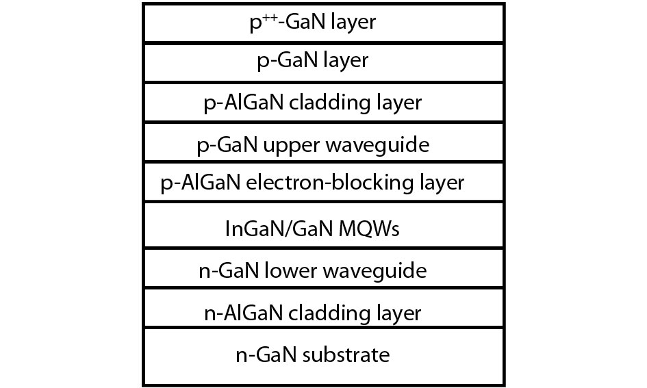
In this work, GaN-based blue-violet LDs are grown on c-plane GaN substrate by metal organic chemical vapor deposition (MOCVD). The trimethylgallium (TMGa) or triethylgallium (TEGa), trimethylaluminum (TMAl), trimethylindium (TMIn), NH3, dicyclopentadienyl magnesium (Cp2Mg), and SiH4 are used as the Ga, Al, In, N, Mg, and Si sources, respectively. The LDs are grown in proper sequence, and the epitaxial structure is shown in Fig. 1. Firstly, a thick n-GaN layer is grown on GaN substrate, and then an n-AlGaN cladding layer (CL), an n-GaN lower waveguide (LWG) layer, InGaN/GaN multi-quantum wells (MQWs), a p-AlGaN electron-blocking layer (EBL), a p-GaN upper waveguide (UWG) layer, a p-AlGaN cladding layer, a p-GaN layer, and a very thin heavily Mg-doped GaN (p++-GaN) layer are grown subsequently. In addition, a 10-μm-wide ridge stripe is formed by dry etching along the <1-100> direction, and a 600- μm-long cavity is fabricated by cleaving along the {1-100} plane after grounding and polishing the GaN substrate to reduce its thickness. The front and rear cleaved cavity facets are coated, and the reflectivity is 10% and 90%, respectively. Moreover, Ti/Pt/Au and Pd/Pt/Au are used to form Ohmic contacts with n-GaN substrate and p-GaN contact layer, respectively.
![]()
Figure 1.Schematic diagram of the epitaxial structure for the GaN-based blue-violet LDs.
3. Results and discussions
The optical spectrum of stimulated emission from the GaN-based LD under CW operation is shown in Fig. 2. It can be seen that the peak wavelength is around 413 nm, and the full width at half maximum (FWHM) of the spectrum is small, i.e. about 0.4 nm. In addition, the inset of Fig. 2 shows the far field pattern of the laser beam when the blue-violet LD illuminates a page of white paper. These results indicate the success in the fabrication of GaN-based blue-violet LD with a lasing wavelength of around 413 nm and CW operated at room temperature.
![]()
Figure 2.(Color online) The optical spectrum of stimulated emission for a GaN-based blue-violet LD. The inset shows the far field pattern of laser beam.
Fig. 3 shows the voltage and optical power of GaN-based blue-violet LD as a function of the forward direct-current (P–I–V) measured at room temperature. It is observed that the optical power increases sharply and lasing starts when the injection current is higher than 87.6 mA. Thus, the threshold current is taken as 87.6 mA, and the corresponding threshold current density is 1.46 kA/cm2. In addition, the peak optical power is larger than 600 mW under an injection current of 800 mA, and the corresponding current density is around 13.33 kA/cm2.
![]()
Figure 3.(Color online) Power–current–voltage (
It is found that the operating voltage under the threshold current, i.e. threshold voltage, is as low as 4.1 V. Such a low threshold voltage may be mainly attributed to our previous works on the improvement of the p-GaN Ohmic contact. In our previous study, we demonstrated the influence of residual carbon impurities in the heavily Mg-doped GaN (p++-GaN) layer on the performance of p-GaN Ohmic contact. A low specific contact resistivity (ρc) of 6.8 × 10⁻⁵ Ω·cm2 is obtained by properly controlling the residual carbon impurity incorporation in the p++-GaN layer[
![]()
Figure 4.(Color online) (a) Current–voltage characteristics obtained for different values of
We have taken the aging experiment to check the lifetime of blue-violet LDs, which is performed at room temperature under a fixed current injection. Fig. 5 shows the optical output power as the function of aging time. It can be seen that the optical power decreases slightly along with the increasing aging time, and the optical power keeps larger than 100 mW as the aging time reaches up to around 1067 h. It demonstrates that the lifetime of GaN-based blue-violet LD is longer than 1000 h under a room-temperature continuous-wave operation. It is noted that output power has declined after the LD operates for the right time, which is supposed to be caused by two reasons. First, the increasing temperature due to the accumulation of the heat process can decrease the slope efficiency and reduce the output power. Second, it may be that there are a few dislocations in GaN-based materials, which can reduce the output power along with increasing aging time. Actually, some necessary technological procedures have been taken in the device fabrication process in order to avoid any failure happening in the early stage of the device operation. We think the long lifetime obtained for the blue-violet LDs is due to our previous work for the improvement of Ohmic contact and material growth, and due to the new LD structure design. In details, first, as mentioned above, an excellent Ohmic contact with a very low specific contact resistance is obtained, which is good for reducing operation voltage and contact resistance. Second, the good p-AlGaN materials are grown by reducing the carbon and hydrogen concentration through controlling the growth conditions[
![]()
Figure 5.Optical power of blue-violet LD as a function of the aging time with a fixed injection current at room temperature.
4. Conclusion
In summary, the continuous-wave GaN-based blue-violet LDs with a lifetime longer than 1000 h operated at room temperature are demonstrated. The blue-violet LDs are grown on c-plane GaN substrate by MOCVD, and a 10 × 600 μm2 ridge waveguide structure device is fabricated. The stimulated emission wavelength of LD is about 413 nm, and the peak optical power is larger than 600 mW. Moreover, the threshold current density and voltage are as low as 1.46 kA/cm2 and 4.1 V, respectively. The fabricated GaN-based blue-violet LDs successfully show a long cw working lifetime.
Acknowledgements
This work was supported by the National Key R&D Program of China (Nos. 2016YFB0401801, 2016YFB0400803), the Science Challenge Project (No. TZ2016003), the National Natural Science Foundation of China (Nos. 61674138, 61674139, 61604145, 61574135, 61574134, 61474142, 61474110), and the Beijing Municipal Science and Technology Project (No. Z161100002116037).
References
[1] N Ruhnke, A Müller, B Eppich et al. Compact deep UV system at 222.5 nm based on frequency doubling of GaN laser diode emission. IEEE Photonic Tech Lett, 30, 289(2018).
[2] G R Goldberg, P Ivanov, N Ozaki et al. Gallium nitride light sources for optical coherence tomography. Gallium Nitride Materials and Devices XII, 101041X(2017).
[3] T Wunderer, J E Northrup, Z Yang et al. Nitride VECSELs as light sources for biomedical applications. CLEO: Applications and Technology, JM3O.1(2013).
[4] B Xue, Z Liu, J Yang et al. Characteristics of III-nitride based laser diode employed for short range underwater wireless optical communications. Opt Commun, 410, 525(2018).
[5] Y F Huang, C T Tsai, Y C Chi et al. Filtered multicarrier OFDM encoding on blue laser diode for 14.8-gbps seawater transmission. J Lightwave Technol, 36, 1739(2018).
[6] U Strauβ, S Brüninghoff, M Schillgalies et al. True-blue InGaN laser for pico size projectors. Gallium Nitride Materials and Devices III, 689417(2008).
[7] E Buckley. Laser wavelength choices for pico-projector applications. J Display Technol, 7, 402(2011).
[8] S Essaian, J Khaydarov. State of the art of compact green lasers for mobile projectors. Opt Rev, 19, 400(2012).
[9] Y Gan, Y Lu, Q Y Xu et al. Compact integrated green laser module for Watt-level display applications. IEEE Photonic Tech Lett, 25, 75(2013).
[10] S Nakamura, M Senoh, S I Nagahama et al. Violet InGaN/GaN/AlGaN-based laser diodes with an output power of 420 mW. Jpn J Appl Phys, 37, L627(1998).
[11] S Nakamura, M Senoh, S I Nagahama et al. InGaN-based multi-quantum-well-structure laser diodes. Jpn J Appl Phys, 35, L74(1996).
[12] M T Hardy, D F Feezell, S P DenBaars et al. Group III-nitride lasers: a materials perspective. Mater Today, 14, 408(2011).
[13] T D Moustakas, R Paiella. Optoelectronic device physics and technology of nitride semiconductors from the UV to the terahertz. Rep Prog Phys, 80, 106501(2017).
[14] J Kim, H Kim, S N Lee. Thermal degradation in InGaN quantum wells in violet and blue GaN-based laser diodes. Curr Appl Phys, 11, S167(2011).
[15] S Masui, Y Nakatsu, D Kasahara et al. Recent improvement in nitride lasers. Gallium Nitride Materials and Devices XII, 101041H(2017).
[16] S P Najda, P Perlin, T Suski et al. AlGaInN laser-diode technology for optical clocks and atom interferometry. Gallium Nitride Materials and Devices XII, 101041L(2017).
[17] S P Najda, S Stanczyk, A Kafar et al. Tapered waveguide high power AlGaInN laser diodes and amplifiers for optical integration and quantum technologies. Quantum Technologies & Quantum Information Science, 104420O(2017).
[18] S P Najda, P Perlin, T Suski et al. GaN laser diodes for high-power optical integration and quantum technologies. Gallium Nitride Materials and Devices XIII, 1053217(2018).
[19] P Chen, D G Zhao, M X Feng et al. A high power InGaN-based blue-violet laser diode array with a broad-area stripe. Chin Phys Lett, 30, 104205(2013).
[20] D G Zhao, D S Jiang, L C Le et al. Performance improvement of GaN-based violet laser diodes. Chin Phys Lett, 34, 017101(2017).
[21] F Liang, D G Zhao, D S Jiang et al. Improvement of Ohmic contact to p-GaN by controlling the residual carbon concentration in p++-GaN layer. J Cryst Growth, 467, 1(2017).
[22] F Liang, D G Zhao, D S Jiang et al. Influence of residual carbon impurities in a heavily Mg-doped GaN contact layer on an Ohmic contact. Appl Opt, 56, 4197(2017).
[23] J Yang, D G Zhao, D S Jiang et al. Investigation on the compensation effect of residual carbon impurities in low temperature grown Mg doped GaN films. J Appl Phys, 115, 163704(2014).
[24] J Yang, D G Zhao, D S Jiang et al. Influence of hydrogen impurities on p-type resistivity in Mg-doped GaN films. J Vac Sci Technol A, 33, 021505(2015).
[25] F Liang, J Yang, D G Zhao et al. Influence of hydrogen impurity on the resistivity of low temperature grown p-Al
[26] J Yang, D G Zhao, D S Jiang et al. Emission efficiency enhanced by reducing the concentration of residual carbon impurities in InGaN/GaN multiple quantum well light emitting diodes. Opt Express, 24, 13824(2016).
[27] F Liang, D G Zhao, D S Jiang et al. Performance enhancement of the GaN-based laser diode by using an unintentionally doped GaN upper waveguide. Jpn J Appl Phys, 57, 070307(2018).

Set citation alerts for the article
Please enter your email address
© Copyright 2018-2021 | Chinese Laser Press. All Rights Reserved 沪ICP备15018463号-20