Junbo Zhu1,2,3, Weiwei Zhang1,*, Ke Li1,4, Bharat Pant1..., Martin Ebert1, Xingzhao Yan1, Mehdi Banakar1, Dehn T. Tran1, Callum G. Littlejohns1, Fuwan Gan2, Graham Reed1 and David J. Thomson1,5|Show fewer author(s)
1Optoelectronics Research Centre, University of Southampton, Southampton SO17 1BJ, UK
2National Key Laboratory of Materials for Integrated Circuits, Shanghai Institute of Microsystem and Information Technology, Chinese Academy of Sciences, Shanghai 200050, China
3University of Chinese Academy of Sciences, Beijing 100049, China
Junbo Zhu, Weiwei Zhang, Ke Li, Bharat Pant, Martin Ebert, Xingzhao Yan, Mehdi Banakar, Dehn T. Tran, Callum G. Littlejohns, Fuwan Gan, Graham Reed, David J. Thomson, "Universal silicon ring resonator for error-free transmission links," Photonics Res. 12, 701 (2024)
Copy Citation Text
【AIGC One Sentence Reading】:We developed a silicon PN junction ring resonator for error-free C band communication at 50 Gb/s, featuring high modulation and detection performance, paving the way for future high-speed all-silicon optical transceiver links.
【AIGC Short Abstract】:We developed a universal silicon PN junction ring resonator for error-free communication links, achieving a 50 Gb/s transmission rate with high modulation and detection performance. This innovative device ensures a low bit error rate, high responsivity, and modulation efficiency, enabling fast and reliable data transmission. Its design eases fabrication challenges and paves the way for future high-speed, all-silicon optical transceiver links.
Note: This section is automatically generated by AI . The website and platform operators shall not be liable for any commercial or legal consequences arising from your use of AI generated content on this website. Please be aware of this.
Abstract
We report the design, fabrication, and characterization of a universal silicon PN junction ring resonator for C band error-free communication links operated up to 50 Gb/s with co-designed optical modulation and detection performance. The universal p-n junction ring device shows co-designed detection responsivity up to 0.84 A/W, in conjunction with a modulation efficiency of and optical modulation extinction ratio, enabling C band 50 Gb/s NRZ communication link with a bit error rate . Individually, the speed of modulation and detection is measured up to 112 Gb/s and 80 Gb/s, respectively. The principle of co-designing the PN junction ring modulator and detector performance required for error-free communication links can significantly ease the fabrication yield challenges of ring structures by reducing the number of types of devices. The principle can also be applied to O band wavelengths. To the best of our knowledge, for the first time, a device of this type has achieved both error-free modulation and detection operation up to 50 Gb/s in the C band individually or in conjugation as an error-free communication link, which paves the way to realize a all-silicon WDM-based error-free optical transceiver link in the future and is essential for future programmable photonics circuits.
1. INTRODUCTION
Over the past decades, the fast-growing bandwidth demand on data centers, artificial intelligence, clouding computing, and Internet of Things has driven the development of silicon photonics [1–3]. Benefiting from mature CMOS manufacturing techniques, silicon photonics integrated circuits have become a promising technology that aims to achieve system-level integration with low power consumption, low cost, small footprint, and high bandwidth. With no alteration to conventional CMOS materials and manufacturing processes, all-silicon optical transmission links have drawn a lot of attention [4].
As two indispensable building blocks of an all-silicon optical transceiver link, enormous efforts have been made to develop high-performance modulators (MODs) and photodetectors (PDs) individually [5–8]. However, the design differences required for PDs and MODs can significantly increase the complexity and the cost of fabrication as well as the electrical circuit design for wavelength control/trimming [9–15] and stabilization in the 300 mm silicon photonics platform [16–18]. Therefore, a universal structure with both high-speed modulation and detection operation will greatly enhance the silicon photonics integration level at low cost and can enrich programmable photonics circuits with more flexibility for light detection and modulation. Having one component that can function as either a modulator or a detector is attractive for a programmable circuit as it means the chip area that is required for would otherwise be needed for dedicated components to serve these functions that can be saved and/or the circuit that can be more versatile to serve a larger number of applications [19,20].
In the early stages, defect-mediated sub-bandgap absorption is observed in general carrier-depletion silicon modulators with optical responsivity below 0.1 A/W and was proposed for optical power monitoring, for which data speed response at 35 Gb/s has been measured [21]. Silicon Mach–Zehnder interferometer (MZI)-type MODs and their straight PN-junction waveguide arm-based PDs have demonstrated error-free transmission links at a signal speed of 10 Gb/s for B2B and 10/20 km fibers [22,23]. Recently, owing to their compact size for co-packaged optics and resonance advantage for WDM links for high bandwidth optical I/O, micro-ring resonator (MR) devices have played a crucial role in the development of high bandwidth density Tb/s communication links. Unlike MZIs, the MR is a good candidate for co-designing optical modulation and detection properties via MR resonance enhancement (RE) effects. Early universal MR devices have shown 44 Gb/s modulation speed with a of 1.7 V · cm [24] and 40 Gb/s detection speed with 48 mA/W responsivity under 8 V bias in the avalanche mode [25]. Photon-assisted tunneling (PAT) for sub-bandgap light detection in silicon PN-doped waveguides was later analyzed in the avalanche mode, where a strong electric field in the depletion region can generate the photon-assisted tunneling current due to impurity-assisted Franz–Keldysh absorption and amplify the generated photocurrent through avalanche multiplication gain, which is much less dependent on the defects in the doped silicon PN junction [26], enabling the MOD and avalanche photodetector (APD) to share the same PN junction and allowing a responsivity as high as 0.53 A/W to be measured in a ring resonator device [27]. In such case, O band 100 Gb/s PAM-4 can be measured with this responsivity benefiting from avalanche gain and a 3 dB OE bandwidth of [27]. A modulation efficiency of and an EO bandwidth 40 GHz have also been achieved in the same device fabricated by using a standard foundry process [28]. A higher OE bandwidth of 35 GHz with a lower responsivity of 0.21 A/W and an EO bandwidth with have also been measured in another universal ring device with customized doping [29,30].
Sign up for Photonics Research TOC. Get the latest issue of Photonics Research delivered right to you!Sign up now
However, the performance of two previous universal MR devices either as a ring detector or modulator is limited and is inferior to the performance of state-of-the-art devices dedicated as either a modulator or detector. Currently, silicon ring PN junction MRs have been reported with impressive performance for individually optimized silicon MR-MODs and MR-PDs in the O band. For example, silicon ring modulators have reached an impressive high-speed operation of 128 Gbaud [31], while silicon ring detectors have been optimized up to 60 Gbaud (38 GHz) with a responsivity of 0.73 A/W [32]. A all-silicon ring-based WDM transceiver with CMOS ICs has demonstrated s per wavelength error-free operation with a nonlinear feed-forward-equalizer (NL-FFE) enabled in the modulation side, and with a post-transimpedance amplifier (TIA) FFE and a decision-feedback-equalizer (DFE) enabled in the detection side by using an individually designed MR-APD and MR-MOD [4].
Now the question comes to specifically how we can achieve a high-performance universal ring device with state-of-the-art performances of the MR-APD and MR-MOD. Additionally, the PAT probability of sub-bandgap light absorption in the C band is weaker than absorption in the O band [26], which raises challenges in developing such a high-performance universal ring in the C band. So far, error-free communication links based on universal PN junction MRs have not been reported. These challenges are addressed here for the first time by co-designing the modulation efficiency of the MR-MOD to relax the MR-APD’s bandwidth and noise for high-performance error-free optical links with low latency for cloud computing and networking in data centers.
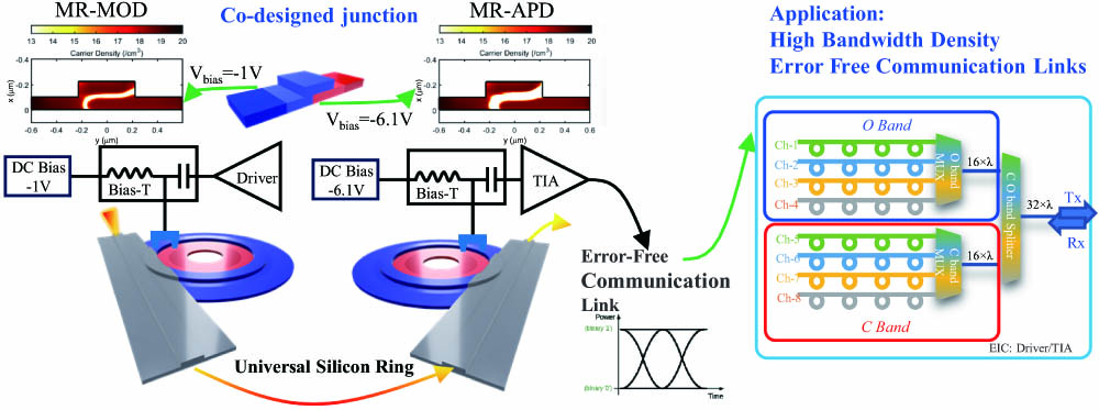
In this work, we report a C band universal silicon PN junction MR with a resonance bandwidth from 1525 to 1565 nm, and designed to perform simultaneously as an APD and an MOD toward an error-free transmission link that is less dependent on the RF driver, TIA, and digital signal processor (DSP) chips. As an optical modulator a of 4.0 V · mm and more than 8 dB modulation extinction ratio (ER) have been achieved with an RF driving voltage of . The photodetection performance shows a high responsivity up to 0.84 A/W before saturation and dark current . The performance for both is comparable with the current state of the art as discussed above. The adopted co-design strategy for an error-free link relies on a large enough modulation ER to overcome its high noise-limited photodetection performance, achieving a bit error rate (BER) of at 40 Gb/s without electrical and optical DSP or filters, and an BER of () at 50 (56) Gb/s with 3 taps FFE at the detection side. This work provides a universal C band silicon PN junction ring resonator design capable of performing as either an MR-APD or an MR-MOD, simplifying fabrication, and supporting error-free communication without DSP techniques for next-generation high-speed all-silicon optical transmission applications.
2. DESIGN
The schematic diagram of the optical transmission link is shown in Fig. 1. The performance of the modulator and detector needs to be co-designed to realize error-free data transmission enabled by the universal MR. Typically, the BER is estimated by and erfc(·) is the complementary error function. Q can be defined as Eq. (1), where and represent the high and low voltage levels of the signal; and are Gaussian approximations of the receiver noise, respectively; is the responsivity of the MR detector; is the average of the received optical power ; and represent the high and low power levels of the modulated optical signal; ER represents the extinction ratio of the modulated optical signal; and () represents the TIA function converting current levels to voltage levels:
Figure 1.Schematic diagram of an error-free transmission link enabled by a universal MR, and its application to scale up for in O and C band for a 1.6 Tb/s error free link (Appendix C).
Under the approximation of Eq. (1) and given the total noise (), the BER performance of an MR-MOD- and MR-APD-based communication link is mainly determined by (1) the input optical power and the of the modulated optical signal, and (2) the responsivity of the MR-APD. The noise from the MR-MOD and MR-APD is also expected to be low enough for TIA circuits to handle the final error-free operation. In this work, the TIA design for low-noise operation is not discussed and the main focus is to develop a high-performance universal silicon PN junction MR for robust error-free communication that is less dependent on signal processing enabled by DSP, TIA, and other electrical or optical filters, etc. Consequently, the optoelectronics properties of the universal ring device as MR-MOD and MR-APD are co-designed to both achieve a high modulation ER at given for the MR-MOD and a high for the MR-APD. For a given and laser power , the average optical power insertion loss () of the MR-MOD is defined as . Therefore, a lower is better. The modulated optical signal after the MR-MOD should be error free before being detected by the MR-APD. When the optical signal is converted into an electrical signal by the MR-APD and TIA, the detected signal’s BER will be also affected by the received power , responsivity , and dark current of the MR-APD.
As a universal ring device for MOD and APD, the co-design is focused on a range of performance metrics: modulation efficiency , responsivity , dark current , and . To engineer these performances, we adopted an L-shape PN junction in a silicon rib waveguide, as shown in Figs. 1 and 2(c), which has a larger overlap area between the depletion region and optical mode than the conventional lateral PN junction, resulting in better modulation and detection efficiency. The universal ring design is based on a 10 μm radius micro-ring structure with an active doping region around 73% of its circumference. The waveguide dimensions are with a 100 nm high slab.
Figure 2.Simulated (a) doping losses, (b) modulation efficiencies, (c) electric field density distribution, and (d) confinement factors of the low doping vertical junction (L-V), medium doping vertical junction (M-V), high doping vertical junction (H-V), and medium doping L-shape junction (L-shape) produced by using Silvaco TCAD and Lumerical.
A larger -factor can result in better responsivity via the resonance enhancement effect, but also limits the optical bandwidth with longer photon lifetime. Here we design the optical 3 dB bandwidth () close to 50 GHz to support error-free high-speed modulation and detection at 50 Gbaud, which means the -factor should be close to or lower than 3800 for resonant wavelengths () around 1550 nm by Eq. (2). Under critical coupling, and both are about 0.94 to meet the -factor value of 3800. The optical waveguide loss () is approximately 12 dB/mm:
The universal MR with L-shape PN junction, as shown in Fig. 1, is also designed to operate with an electrical bandwidth of 50 GHz as typically required for high signal integrity operation and 50 Gbaud error-free data transmission. By the lumped bandwidth model of Eq. (3), the ring junction capacitance () has an upper limit value of about 64 fF when only considering the 50 Ω source impedance (). Considering 73% region of the designed MR is doped as an active PN junction, the capacitance per length limit of the PN junction cross section () is 1.4 fF/μm:
The doping profile of the PN junction was optimized to achieve high modulation and detection efficiency with the constraints of the discussed parameters, 12 dB/mm optical waveguide loss , and 1.4 fF/mm PN junction capacitance . The modulation and detection, relying on the plasma dispersion effect [33] and the PAT effect [26], both occur in the depletion region, the width of which is given by where is the dielectric permittivity of silicon, is the electron charge, and is the p- and n-type doping concentrations. is the difference between the built-in voltage and bias voltage. The width of the depletion region is proportional to the square root of the doping concentration , as shown by Eq. (4). The effective absorption coefficient of PAT () is related to the confinement/overlap factor () of the optical mode in the depletion region. is the PAT absorption coefficient. A larger doping concentration provides more carriers for modulation and therefore increasing the doping level provides an enhancement of the modulation efficiency, but will decrease the width of the depletion region, which results in a reduction of the photon absorption efficiency.
To find a good trade-off between and photon absorption efficiency under all of the above restrictions, the PN junction is designed, with simulated key parameters (8–10 dB/mm), (0.12–0.29), and (4–5.8 V · mm), as shown in Fig. 2. We also compared the simulated parameters (, , ) of the proposed device (medium doping , L-shape) with devices having vertical PN junctions at different doping levels: lower doping (, L-V), medium doping (, M-V), and higher doping (, H-V). The p-type region of the vertical PN junction is optimized to be 20 nm wider than the n-type region, because free holes have a smaller absorption and a larger shift of the real part of the refractive index than free electrons in silicon.
As shown in Fig. 2(c), the L-shape structure has an times wider depletion area while it still keeps a narrow depletion width (), which is important for high-speed detection and modulation. From Figs. 2(a) and 2(b), the L-shape structure exhibits excellent performance with resonable doping loss. The L-shape PN junction also shows a better spatial overlap between the depletion region and the optical mode profile, as shown in Fig. 2(d), which will significantly enhance the total photon absorption efficiency via PAT. These results suggest that the proposed universal ring resonator with an L-shape PN junction possesses excellent performance in terms of modulation and detection.
3. DC CHARACTERIZATION
The device fabrication is summarized in Appendix A, and the radius is 10 μm. The measured transmission spectrum is shown in Fig. 3(a), in which the -factor is about 4200, the DC ERs are , and the free spectral range (FSR) is . The fabricated devices show high insertion losses from grating to grating, about 20 dB, caused by modifications to the standard foundry process flow inducing extra grating losses. This can be rectified in the future by using a different grating coupler design. The parameters of the ring resonator are then extracted. The self-coupling coefficient (r) and round-trip optical ring resonator attenuation () are extracted as . Thus, the corresponding cavity resonance enhancement RE [34] is calculated as . The measured phase shift efficiency of the micro-ring is shown in Fig. 3(b), which shows a good agreement with simulation results.
Figure 3.Measured (a) transmission spectrum and (b) phase change efficiency of 10 μm radius MR.
The measured MR-MOD resonance shifts with applied bias are shown in Fig. 4(a). With a swing, a large DC ER of 14 dB can be achieved with a one level IL of about 4 dB, as shown in Fig. 4(b). The PAT probability is expressed as [26,35] where is the electron’s effective mass in silicon, is the potential barrier height, and is the effective barrier width. The simulated electrical field of the Si L-shape PN junction at 0 and is shown in Fig. 4(c). By increasing the reverse bias voltage, the electrical field becomes stronger and the depletion width () becomes larger, which increases the PAT effective absorption coefficient with larger overlap between the optical mode and depletion region, also as shown in Fig. 4(c). From the simulated energy bandgap in Fig. 4(c), decreases from at 0 V to at . The reduced can increase the tunneling probability exponentially by Eq. (5). In addition, the maximum electrical field () at is sufficient to trigger impact ionization in silicon for avalanche gain. Therefore, the measured responsivity at the resonant wavelength [Fig. 4(d)] exhibits an exponential-like increase at high reverse bias voltages due to the exponential increase of PAT absorption and avalanche gain. With the help of resonant enhancement, 0.84 A/W responsivity has been measured when the bias voltage is and the input optical power is before reaching saturation.
Figure 4.Measured (a) DC electro-optical wavelength shifts and (b) DC ER versus one level losses with different voltage swings. (c) Simulated conduction and valence band diagrams of the Si L-shape PN junction at different bias voltages. (d) Measured responsivity versus bias voltage.
While working as an APD, the measured dark current and total current of the MR-APD with different input optical powers are shown in Fig. 5(a). The dark current is about 700 nA at . As shown in Figs. 5(b) and 5(c), the responsivity decreases with injected optical power, which can be attributed to avalanche gain saturation in APDs [36]. From Fig. 5(d), we can see that even though the responsivity decreases with optical power, the current at high voltages still increases significantly, showing a high photocurrent of 0.3 mA with around 5.1 dBm of input optical power at .
Figure 5.Measured (a) dark and total current versus bias voltage for different optical input powers, (b) responsivity versus bias voltage at different input optical powers, (c) responsivity versus input optical power at different bias voltages, (d) total current at different voltages and optical input powers.
The bandwidth of the depletion ring is first estimated by high-speed data transmission experiments. 80 Gb/s optical modulation eye diagrams (without pattern averaging) and 50 Gb/s optical detection eye diagrams (without pattern averaging) have been measured to determine whether their bandwidths are above 35 GHz (Appendix B). To be noted, when operating as an MR-APD, the eye diagram is limited by intrinsic noise and the performance of a 40 GHz lithium niobate MZI modulator (LN MZI-MOD) used to generate the high-speed optical signal, for which the 80 Gb/s optical eye-diagram is closed (Appendix B) and therefore extra FFE taps are needed for the MR-APD measurement. The detailed test setup and testing process are summarized in Appendix B.
High-performance detection by an MR-APD with a BER level around has been achieved at lower data rates without the help of using dedicated low-noise TIAs and electrical and optical filters in the detection side. The measured 40 Gb/s, 50 Gb/s, and 56 Gb/s eye diagrams of the MR-APD with input bus waveguide optical power of at 6.1 bias are shown in Figs. 6(a)–6(c). BERs of at 40 Gb/s (without FFE), at 50 Gb/s (3 taps FFE), and at 56 Gb/s (3 taps FFE) are measured. To reach a BER of or even lower at 40 Gb/s, the required optical power from the transmitter (Tx) (average power of the modulated signal from the LN MZI-MOD) is 6 dBm and the required optical modulation ER is about 7.1 dB. Despite the dark current of and excess noise of Si, the receiver (Rx) side has also tolerated the amplified spontaneous emission noise from the erbium-doped fiber amplifier (EDFA) (with no optical filters) required due to the high IL of the grating couplers. And neither noise filter was enabled in the electrical port of the digital communication analyzer. In addition, a linear amplifier was used instead of a TIA for the Rx. Therefore, the optical sensitivity of the Rx can be further improved in future work by overcoming high grating losses and integration with dedicated electrical Rx circuits (TIA, filter, etc.).
Figure 6.Measured eye diagrams of MR-APD at bit rates of (a) 40 Gb/s, , and MOD ; (b) 50 Gb/s, , and MOD , with 3 taps FFE; (c) 56 Gb/s, , and MOD , with 3 taps FFE. Eye diagrams of MR-MOD at bit rates of (d) 40 Gb/s, ; (e) 50 Gb/s, ; (f) 56 Gb/s, . Eye diagrams of LN MZI-MOD at bit rates of (g) 40 Gb/s, ; (h) 50 Gb/s, ; (i) 56 Gb/s, .
For comparison, by sending the same modulated optical signal from the LN MZI-MOD to the reference PD of the 65 GHz optical detector within the Keysight 86116C-40 (with noise filter off, the sensitivity is and when the filter turned on at 40 Gb/s, the characteristic RMS noise is 36 μW), the required optical power is about 2 dBm to reach a BER level of , as shown in Fig. 7. Under the same conditions, to reach a BER of at 50 Gb/s, the required optical power in the bus waveguide of the MR-APD is about 6.2 dBm. The BER performance of the MR-MOD is also compared with the LN-MZI-MOD in Fig. 7. At 40 Gb/s and 50 Gb/s, the measured optical power VS BER is similar, and both can reach high optical and very low for data rates 40–56 Gb/s. The MR-MOD is biased at and driven with an RF voltage of . At 40 Gb/s, the BER for MR-APD reaches the order of when the received optical power is 6 dBm and the input ER is 7 dB. The optical power can be reduced to 4.4 dBm when 3 taps FFE is enabled. At 50 Gb/s, the BER of the MR-APD is of the order of with 3 taps FFE enabled and 7 dBm optical power.
Figure 7.Measured (a) 40 Gb/s and (b) 50 Gb/s NRZ BER with different optical power for the MR-APD, MR-MOD, and LN MZI-MOD.
When the bit rate exceeds 40 Gb/s, the BER performance of the MR-APD is mainly limited by the degraded modulated optical signal of the LN MZI-MOD. As illustrated in Fig. 8, the SNR of the modulated optical signal generated by the LN MZI-MOD quickly rolls off from 10 to 5 when the bit rate increases from 40 Gb/s to 64 Gb/s, which is the fundamental bottleneck for this work to demonstrate error-free detection beyond 50 Gb/s. We have also measured comparable SNR (in Fig. 8) and ER/BER (in Fig. 6) performance of the MR-MOD in comparison with the LN MZI-MOD. The of the high ER eye diagrams measured in Fig. 6 can be reduced to as low as 6 dB. These results demonstrate that the MR-MOD can produce high-quality modulated optical signals comparable to those generated by the LN MZI-MOD for supporting the error-free detection.
Figure 8.Measured SNR of the MR-MOD and LN MZI-MOD at different bit rates with the same ER of 8 dB.
Finally, we show the impact of co-designing the MR-APD and MR-MOD on the BER performance of the Rx. As shown in Figs. 9(a)–9(c), the measured BER of the Rx at a data rate of 40 Gb/s is strongly dependent on the Tx ER. The BER significantly decreases from to when the ER increases from 4 dB to 8.2 dB and the received optical power is kept at 6 dBm. Such a high ER performance has been co-designed and achieved for the MR-MOD as shown in Fig. 6. Based on the performance analysis of the MR-APD and the MR-MOD (6 dB ), an error-free communication link can be built by simply using the co-designed universal depletion ring resonator with coupled optical power of about 12 dBm.
Figure 9.Measured eye diagrams of the MR-APD at 40 Gb/s and with (a) MOD and (b) MOD ; (c) 40 Gb/s NRZ BER of the MR-APD decreases with an increasing modulated optical ER of the LN MZI-MOD.
In Table 1, we summarize the measured performance and compare with state-of-the-art reports of CMOS-SiPh transceiver demonstrations. Despite not being integrated with a CMOS TIA and driver, our presented results clearly stand out in terms of both modulation and detection performance (Table 2) as well as higher-speed error-free operation with less overhead coding for forward-error correction. This can reduce the requirement for electronic devices to reconstruct the original bit stream and facilitate large-scale integration with low power consumption and lower latency. The current unpackaged approach suffers for optical noise from the EDFA, and the sensitivity of the Keysight 86116C-40 (with noise filter off) increases to 2 dBm from when the noise filter turned on at 40 Gb/s, which means there is a potential for 7 dB of laser power reduction if the MR-APD-based Rx performances are compared with the Rx of the Keysight 86116C-40. Current state-of-the-art TIA design based on 16 nm FinFET technology only requires μ (peak-peak) current amplitude for error-free operation when integrated with a GeSi waveguide PD [39]. For our co-designed MR-APD, it shows a current amplitude of μ (peak-peak) when the input optical power is switched from to , as shown in Fig. 5(d). Therefore, it is possible to realize a low-sensitivity MR-APD Rx at about with the help of a dedicated TIA and further optimization of the Si APD, and the optical power budget of the laser can be reduced to less than 0 dBm when only considering the insertion loss from the MR-MOD, which is about 12 dB lower than the current unpackaged demonstration where the Rx side utilized a linear RF amplifier. All passive integration should also be improved with negligible insertion loss. Beyond the optical co-design approach explained in this work, co-design of the Tx and Rx electronics circuits can also further reduce the link power budget toward higher-speed operation with lower power consumption in the future.
Performance Summary and Comparison between State-of-the-Art Ring-Based CMOS Optical Links and Our Work
[37]-2012
[38]-2019
[39]-2020
[4]-2021
[40]-2023
This Work
Integration
130 nm SOI driver, TIA
14 nm FinFET driver, TIA
16 nm FinFET driver, TIA
28 nm CMOS driver, TIA
CMOS driver, TIA
Unpackaged
Laser power
7.6 dBm
/
6 dBm
8.1 dBm
12 dBm
Wavelength
C band
O band
C band
O band
O band
C band
Tx MOD
Ring
Ring
GeSi EAM
Ring
Ring
Ring
Tx driver
2 V
1.4 V
1.8 V
2.6 V
1.3 V
2.5 V
Tx BER
25 Gb/s w/pre-emphasis
40 Gb/s
50 Gb/s w/pre-equalization
50 Gb/s
40 Gb/s
56 Gb/s
Tx ER
6.9 dB
4.6 dB
4.3 dB
5.3 dB
Rx PD
Ge PD
Ge PD
GeSi PD
Si ring PD
Ge PD
Si ring PD
PD responsivity
0.8 A/W
1 A/W
1 A/W
0.23 A/W
0.94 A/W
0.84 A/W
Rx BER
25 Gb/s
38 Gb/s
50 Gb/s w/CTLE
50 Gb/sFFE + DFE
40 Gb/s
40 Gb/s
50 Gb/s with 3 taps FFE
Performance Summary and Comparison between State-of-the-Art Universal Devices and Our Work
Type
Responsivity (A/W)
()
Bandwidth (GHz)
Si-ring [21]
/
Si-ring [24,25]
1.7
20
Si-MZI [22,23]
0.54
0.81
26
Si-ring [27,28]
0.53
1
25.5
Si-ring [29]
0.21
0.825
35
Our work
0.84
0.4
6. CONCLUSION
In this work, we have demonstrated a silicon depletion universal ring with co-designed high-performance properties of optical modulation (4 V · mm) and optical detection ( 0.84 A/W), allowing error-free communication links operating up to 50 Gb/s. Based on our current demonstrated results, the MR-APD needs around 6 dBm (4 mW) input optical power and an optical ER of 7 dB to generate OE conversion with a , indicating that the link requires a coupled laser power (16 mW) in consideration of 6 dB due to the MR-MOD. The co-designed MR-MOD can fulfill this high optical power operation with low and high modulation . In the future, integration with a CMOS driver with better signal integrity and SNR for the MR-MOD Tx and also with dedicated low-noise TIA circuits for the MR-APD will significantly improve the BER of the transmission link [4] beyond 50 Gb/s. Our work proves the principle of using a universal ring device to form a high-speed error-free communication link in the optical C band, which can be also applied to the O band and thus provides a simplified all-silicon universal ring resonator solution for WDM-based error-free communication links beyond 1.6 Tb/s (see Appendix C) in the future and for programmable photonics circuits configured for multi-function purpose.
Acknowledgment
Acknowledgment. D. J. Thomson acknowledges funding from the Royal Society for his University Research Fellowship.
APPENDIX A: FABRICATION
The fabrication of the silicon depletion ring resonators is based on 8-inch (1 inch = 2.54 cm) SOI wafers by using the open-source, license-free silicon photonics prototyping foundry CORNERSTONE [41]. The fabrication process flow can be found in Ref. [41], and the doping process to form the L-shape PN junction is customized. In the fabrication process, boron is initially doped into the 220 nm thick silicon active region, and then the waveguide is etched. Afterwards, phosphorus doping is carried out with a tilt angle of 45 deg and six equal rotations between 0 and 360 deg to form the L-shape doping profiles all around the resonators, as depicted in Fig. 10. The and targeted at a doping level of were added layer.
Figure 10.(a)–(c) Schematic diagrams of doping micro-ring to form L-shape PN junctions with 6 rotations.
For the performance measurement of the MR-APD, CW laser light first went through a polarization controller (PC), and then was modulated by a 40 Gb/s LN MZI-MOD. The modulated optical signal was then amplified with a two-stage EDFA before it was coupled to the MR-APD through a second PC. The photocurrent signal was then collected by a combination of a 67 GHz RF open probe, a 64 GHz bias tee, and a 60 GHz RF linear amplifier, and then sent to the 80 GHz electrical port of a Keysight digital communication analyzer (DCA-X 86100D + Agilent 86116C-040), as shown in Appendix B, Fig. 11(a). The BER characterization is done in jitter mode. The eye diagrams and BER characterization of the LN-MZM and MR-MOD were detected by the 65 GHz optical detector of the Keysight DCA with the SIRC and filter off, as shown in Appendix B, Fig. 11(b). Two PRBS11 data are generated and sent to the MUX. The measured eye diagrams of LN-MZI-MOD, MR-APD, MR-MOD, and RF signal are shown in Fig. 12.
Figure 11.Experimental setup for eye diagram and BER measurements of (a) MR-APD and (b) MR-MOD.
Figure 12.Measured eye diagrams of (a) LN-MZI-MOD at 50 Gb/s, (b) MR-APD at 50 Gb/s, (c) LN-MZI-MOD at 80 Gb/s, (d) MR-APD at 80 Gb/s with 5 taps FFE and eye average, (e) RF signal before the RF probe at 80 Gb/s, (f) MR-MOD at 80 Gb/s, (g) RF signal at 112 Gb/s, (h) MR-MOD at 112 Gb/s with 5 taps FFE in the DCA.
APPENDIX C: WAVELENGTH-DIVISION (De)MULTIPLEXING FOR 1.6?Tb/s
The envisioned 1.6 Tb/s Tx or Rx can be achieved by using four FSR windows of MR-APD/MOD in the O and C bands, as shown in Fig. 13, which means four wavelengths are operating in one FSR range about 10 nm, which is large enough for supporting error-free operations [4]. The passive (de)multiplexing used for dividing wide band into four wavelength windows with 10 nm separation can be achieved with low loss [42]. And the demonstrated passive (de)multiplexing for the O/C band also shows low insertion loss () and high extinction ratio () [43]. These settings of 1.6 Tb/s ring arrays guarantee fully utilizing the lasers, modulators, and detectors developed for O/C bands, and cross talk between different rings and wavelength bands is largely suppressed. Therefore, error-free operation is possible to achieve in the future.
Figure 13.MR’s four FSR channels have to be matched with MUX/De-MUX channels. Four MRs operate in each channel, and 16 in total for the C and O band.
[4] H. Li, Z. Xuan, R. Kumar. A 4 × 50 Gb/s all-silicon ring-based WDM transceiver with CMOS IC. European Conference on Optical Communication (ECOC), 1-3.
[7] M. Sakib, P. Liao, R. Kumar. A 112 Gb/s all-silicon micro-ring photodetector for datacom applications. Optical Fiber Communications Conference and Exhibition (OFC), 1-3.
[17] T. Horikawa, D. Shimura, H. Okayama. Resonant wavelength variation modelling for microring resonators based on fabrication deviation analysis. European Conference on Optical Communication (ECOC), 1-3(2017).
[18] P. Le Maître, J. F. Carpentier, C. Baudot. Impact of process variability of active ring resonators in a 300 mm silicon photonic platform. European Conference on Optical Communication (ECOC), 1-3(2015).
[22] K. Goi, N. Ishikura, H. Ishihara. Low-voltage silicon Mach-Zehnder modulator operating at high temperatures without thermo-electric cooling. Optical Fiber Communications Conference and Exhibition (OFC), 1-3(2015).
[29] X. Xiao, L. Wang, J. Liu. Silicon microring-based modulators and photodetectors beyond 100 Gbaud. 27th OptoElectronics and Communications Conference (OECC) and 2022 International Conference on Photonics in Switching and Computing (PSC), 1-3(2022).
[31] M. Sakib, P. Liao, C. Ma. A high-speed micro-ring modulator for next generation energy-efficient optical networks beyond 100 Gbaud. CLEO: Science and Innovations, SF1C-3(2021).
[32] Y. Yuan, Y. Peng, Z. Huang. An O-band all-silicon microring avalanche photodiode with >38 GHz RF bandwidth. IEEE Silicon Photonics Conference (SiPhotonics), 1-2(2023).
[38] D. Guermandi, L. Bogaerts, M. Rakowski. TSV-assisted hybrid FinFET CMOS — silicon photonics technology for high density optical I/O. 45th European Conference on Optical Communication (ECOC), 1-4(2019).
[40] Y. Ban, M. Kim, P. De Heyn. Highly optimized O-band Si ring modulators for low-power hybrid CMOS-SiPho transceivers. Optical Fiber Communications Conference and Exhibition (OFC), 1-3(2023).
Junbo Zhu, Weiwei Zhang, Ke Li, Bharat Pant, Martin Ebert, Xingzhao Yan, Mehdi Banakar, Dehn T. Tran, Callum G. Littlejohns, Fuwan Gan, Graham Reed, David J. Thomson, "Universal silicon ring resonator for error-free transmission links," Photonics Res. 12, 701 (2024)
 AI Video Guide
  AI Picture Guide
 AI One Sentence