• Journal of Semiconductors
  • Vol. 45, Issue 1, 012503 (2024)
Jun Fang1、2, Fan Zhang2, Wenxian Yang2、*, Aiqin Tian2, Jianping Liu2, Shulong Lu2, and Hui Yang2、**
Author Affiliations
  • 1School of Nano-Tech and Nano-Bionics, University of Science and Technology of China, Hefei 230026, China
  • 2Suzhou Institute of Nano-Tech and Nano-Bionics, Chinese Academy of Sciences, Suzhou 215123, China
  • show less
    DOI: 10.1088/1674-4926/45/1/012503 Cite this Article
    Jun Fang, Fan Zhang, Wenxian Yang, Aiqin Tian, Jianping Liu, Shulong Lu, Hui Yang. Electrical properties and structural optimization of GaN/InGaN/GaN tunnel junctions grown by molecular beam epitaxy[J]. Journal of Semiconductors, 2024, 45(1): 012503 Copy Citation Text show less
    (Color online) (a) Schematic diagram of the device structure including GaN/InGaN/GaN TJ. (b) Equivalent circuit diagram of the device.
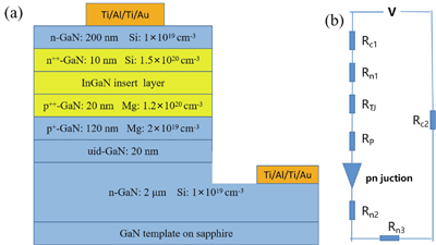
    Fig. 1. (Color online) (a) Schematic diagram of the device structure including GaN/InGaN/GaN TJ. (b) Equivalent circuit diagram of the device.
    (Color online) XRD ω−2θ patterns of the three samples (a) S1 , (b) S2 , (c) S3. The black curve represents the experimental curve, while the red curve represents the simulation curve.
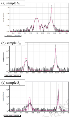
    Fig. 2. (Color online) XRD ω−2θ patterns of the three samples (a) S1 , (b) S2 , (c) S3. The black curve represents the experimental curve, while the red curve represents the simulation curve.
    (Color online) Surface AFM images of the three samples (a) S1, (b) S2, (c) S3.
    Fig. 3. (Color online) Surface AFM images of the three samples (a) S1, (b) S2, (c) S3.
    HRTEM image of the tunnel junction.
    Fig. 4. HRTEM image of the tunnel junction.
    (Color online) (a) I–V curves of the samples, the doping concentration at the TJ of the samples varies, and (b) the change of differential resistance at forward current density.
    Fig. 5. (Color online) (a) IV curves of the samples, the doping concentration at the TJ of the samples varies, and (b) the change of differential resistance at forward current density.
    (Color online) (a) I–V curves of the samples, In content of the InGaN layer at the tunnel junction changes, (b) the change of differential resistance at forward current density.
    Fig. 6. (Color online) (a) IV curves of the samples, In content of the InGaN layer at the tunnel junction changes, (b) the change of differential resistance at forward current density.
    (Color online) I–V curves of the samples, thickness of InGaN layer at tunnel junction varies.
    Fig. 7. (Color online) IV curves of the samples, thickness of InGaN layer at tunnel junction varies.
    (Color online) I–V curves of the samples, doping in InGaN layers at tunnel junctions changes.
    Fig. 8. (Color online) IV curves of the samples, doping in InGaN layers at tunnel junctions changes.
    p++-GaN: 20 nm (1020 cm−3)Insert layer InGaNn++-GaN: 10 nm (1020 cm−3)
    Sample AMg: 1p++-In0.1Ga0.9N: 3 nmMg: 1 × 1020 cm−3Si: 0.5
    Sample BMg: 1.2p++-In0.1Ga0.9N: 3 nmMg: 6 × 1020 cm−3Si: 1.5
    Sample CMg: 1.2 p++-In0.25Ga0.75N: 3 nmMg: 6 × 1020 cm−3Si: 1.5
    Sample DMg: 1.2p++-In0.35Ga0.65N: 3 nmMg: 6 × 1020 cm−3Si: 1.5
    Sample EMg: 1.2No InGaN insert layerMg: 6 × 1020 cm−3Si: 1.5
    Sample FMg: 1.2 Uid-In0.35Ga0.65N: 3 nmSi: 1.5
    Sample GMg: 1.2 Uid-In0.35Ga0.65N: 5 nmSi: 1.5
    Sample HMg: 1.2 n-In0.35Ga0.65N: 3 nmSi: 2 × 1019 cm−3Si: 1.5
    Table 1. The specific structural parameters of GaN/InGaN/GaN TJ.
    Jun Fang, Fan Zhang, Wenxian Yang, Aiqin Tian, Jianping Liu, Shulong Lu, Hui Yang. Electrical properties and structural optimization of GaN/InGaN/GaN tunnel junctions grown by molecular beam epitaxy[J]. Journal of Semiconductors, 2024, 45(1): 012503
    Download Citation