• Photonics Research
  • Vol. 8, Issue 6, 864 (2020)
Zhongjin Lin, Tigran Dadalyan, Simon Bélanger-de Villers, Tigran Galstian, and Wei Shi*
Author Affiliations
  • Department of Electrical and Computer Engineering, Centre for Optics, Photonics and Laser (COPL), Université Laval, Québec, Québec G1V 0A6, Canada
  • show less
    DOI: 10.1364/PRJ.385008 Cite this Article Set citation alerts
    Zhongjin Lin, Tigran Dadalyan, Simon Bélanger-de Villers, Tigran Galstian, Wei Shi. Chip-scale full-Stokes spectropolarimeter in silicon photonic circuits[J]. Photonics Research, 2020, 8(6): 864 Copy Citation Text show less
    Schematic of the proposed spectropolarimeter. The black arrows point to the propagating direction of light. SPS, surface polarization splitter; PA, polarization analyzer; Si-DMRS, our silicon dual-microring resonator spectrometer; PDi, Ge photodetector of the ith Si-DMRS.
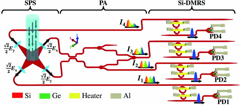
    Fig. 1. Schematic of the proposed spectropolarimeter. The black arrows point to the propagating direction of light. SPS, surface polarization splitter; PA, polarization analyzer; Si-DMRS, our silicon dual-microring resonator spectrometer; PDi, Ge photodetector of the ith Si-DMRS.
    Principle of the proposed Si-DMRS. FSR1(2) in the left side is the free spectral range of the single microring; the subscript 1(2) indicates the first (second) microring of the SDMR. FSR in the right side is the extended free spectral range of the SDMR.
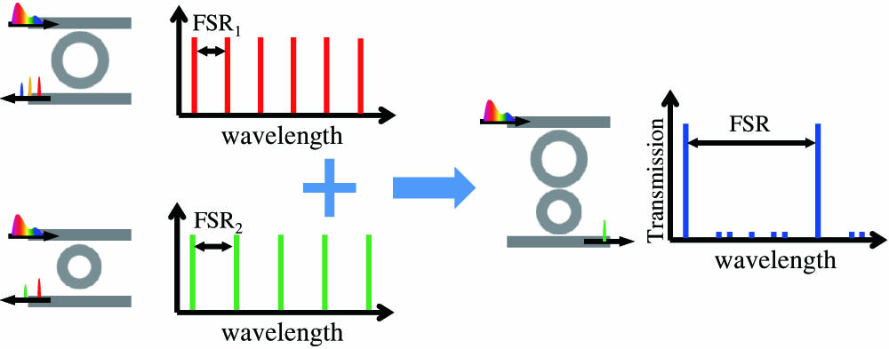
    Fig. 2. Principle of the proposed Si-DMRS. FSR1(2) in the left side is the free spectral range of the single microring; the subscript 1(2) indicates the first (second) microring of the SDMR. FSR in the right side is the extended free spectral range of the SDMR.
    Image of the fabricated spectropolarimeter. (a) The prototype of the fully packaged, plug-and-play spectropolarimeter with a ribbon cable for control and signal readout. (b) The optical micrograph of the fabricated chip before being packaged. (c), (d), and (e) are the SEM images of the Si layer of the SPS, BDC, and SDMR, respectively. The inset in (d) presents the asymmetric-waveguide-based phase control section of the BDC for a broadband operation. SPS, surface polarization splitter; PA, polarization analyzer; Si-DMRS, our silicon dual-microring resonator spectrometer.
    Fig. 3. Image of the fabricated spectropolarimeter. (a) The prototype of the fully packaged, plug-and-play spectropolarimeter with a ribbon cable for control and signal readout. (b) The optical micrograph of the fabricated chip before being packaged. (c), (d), and (e) are the SEM images of the Si layer of the SPS, BDC, and SDMR, respectively. The inset in (d) presents the asymmetric-waveguide-based phase control section of the BDC for a broadband operation. SPS, surface polarization splitter; PA, polarization analyzer; Si-DMRS, our silicon dual-microring resonator spectrometer.
    Dual-MR characterization. (a) Optical micrography of a Si-DMRS. (b), (c) The experimental transmission spectra from the drop port of the SDMR. (d) Relation between resonance wavelength and heating power on the heaters of MR1 (red square) and MR2 (blue square). (e) The experimental transmission spectra of the drop port for the resonance wavelength from 1530 nm to 1579 nm.
    Fig. 4. Dual-MR characterization. (a) Optical micrography of a Si-DMRS. (b), (c) The experimental transmission spectra from the drop port of the SDMR. (d) Relation between resonance wavelength and heating power on the heaters of MR1 (red square) and MR2 (blue square). (e) The experimental transmission spectra of the drop port for the resonance wavelength from 1530 nm to 1579 nm.
    Broadband spectrum reconstruction with the Si-DMRS. Solid black line is the spectrum recorded by a commercial OSA. The dotted lines are the measured results of the Si-DMRS over a week using the same calibration.
    Fig. 5. Broadband spectrum reconstruction with the Si-DMRS. Solid black line is the spectrum recorded by a commercial OSA. The dotted lines are the measured results of the Si-DMRS over a week using the same calibration.
    On-chip spectropolarimeter characterization. (a) Schematic of the CLC sample. (b) Normalized Stokes spectra of the CLC sample, with a linear polarization input, measured by a commercial benchtop instrument (dotted lines) and our on-chip spectropolarimeter (solid lines).
    Fig. 6. On-chip spectropolarimeter characterization. (a) Schematic of the CLC sample. (b) Normalized Stokes spectra of the CLC sample, with a linear polarization input, measured by a commercial benchtop instrument (dotted lines) and our on-chip spectropolarimeter (solid lines).
    (a) Schematic of the SPS. The parameters Λ and D are the period and diameter of the hole, respectively. (b) The simulated transmission spectrum of the SPS.
    Fig. 7. (a) Schematic of the SPS. The parameters Λ and D are the period and diameter of the hole, respectively. (b) The simulated transmission spectrum of the SPS.
    (a) Schematic of the SDMR. t1,(2,3) and κ1,(2,3) are normalized transmission and cross-coupling coefficients, respectively. (b) The simulated transmission spectra of the drop port in the case of κ2=0.005, κ2=0.015, and κ2=0.040 when the resonant wavelength is near 1550 nm.
    Fig. 8. (a) Schematic of the SDMR. t1,(2,3) and κ1,(2,3) are normalized transmission and cross-coupling coefficients, respectively. (b) The simulated transmission spectra of the drop port in the case of κ2=0.005, κ2=0.015, and κ2=0.040 when the resonant wavelength is near 1550 nm.
    (a) Cross-sectional schematic of the Ge-PD. (b) I-V curve in darkness. (c) Photocurrent as a function of optical power for the bias voltage of −4 V.
    Fig. 9. (a) Cross-sectional schematic of the Ge-PD. (b) I-V curve in darkness. (c) Photocurrent as a function of optical power for the bias voltage of 4  V.
    (a) Schematic of the electric connections. (b) The flowchart of searching the corresponding (Ui1, Ui2) for each wavelength. Ui1 and Ui2 are the power applied to first and second MRs of the ith SDMR, respectively. PDi means the photodetector of the ith SDMR. IPDi is the current read from the PDi.
    Fig. 10. (a) Schematic of the electric connections. (b) The flowchart of searching the corresponding (Ui1, Ui2) for each wavelength. Ui1 and Ui2 are the power applied to first and second MRs of the ith SDMR, respectively. PDi means the photodetector of the ith SDMR. IPDi is the current read from the PDi.
    Photocurrent as a function of U11 and U12 at a wavelength of 1562 nm.
    Fig. 11. Photocurrent as a function of U11 and U12 at a wavelength of 1562 nm.
    (a)–(d) are the calibrated heating powers of MRi1 (red) and MRi2 (blue) for each spectral channel.
    Fig. 12. (a)–(d) are the calibrated heating powers of MRi1 (red) and MRi2 (blue) for each spectral channel.
    Experiment setup for calibrating the synthesis matrix or characterizing a chiral material. HWP, half-wave plate; QWP, quarter-wave plate; SMU, source measure unit used for reading the current from the photodetector.
    Fig. 13. Experiment setup for calibrating the synthesis matrix or characterizing a chiral material. HWP, half-wave plate; QWP, quarter-wave plate; SMU, source measure unit used for reading the current from the photodetector.
    Zhongjin Lin, Tigran Dadalyan, Simon Bélanger-de Villers, Tigran Galstian, Wei Shi. Chip-scale full-Stokes spectropolarimeter in silicon photonic circuits[J]. Photonics Research, 2020, 8(6): 864
    Download Citation