Abstract
Tunable optical delay lines are one of the key building blocks in optical communication and microwave systems. In this work, tunable optical delay lines based on integrated grating-assisted contradirectional couplers are proposed and experimentally demonstrated. The device performance is comprehensively improved in terms of parameter optimization, apodization analysis, and electrode design. Tunable group delay lines of 50 ps at different wavelengths within the bandwidth of 12 nm are realized with a grating length of 1.8 mm. Under thermal tuning mode, the actual delay tuning range is around 20 ps at 7.2 V voltage. At last, a new scheme adopting an ultra-compact reflector for doubling group delay is proposed and verified, achieving a large group delay line of 400 ps and a large dispersion value up to within bandwidth of 12 nm. Under thermal tuning mode, the actual delay tuning range is around 100 ps at 8 V voltage.1. INTRODUCTION
Optical delay lines have wide applications in optical communication and microwave photonics systems [1–8]. In optical communication, the main functions of optical delay lines cover signal synchronization, optical buffers, time-division multiplexing, and so forth. In microwave photonics systems, the most eye-catching application of phased array antennas highly relies on the beam-forming technology, which is usually controlled by the array of true-time delay lines.
In general, there are two approaches to the physical implementation of optical delay lines. The most direct and easiest approach for tunable group delay is changing the optical physical distance [9]. For instance, typical schemes are dependent on the selection of long or short delay paths in each stage by Mach–Zehnder interferometer switches [10–12]. Recently, a novel scheme of hexagonal integrated waveguide mesh configurations was proposed for the implementation of compact discrete and continuous optical true-time delay lines [13]. Although this approach is very intuitive and simple, the implementation of long time delays comes at the cost of large dimension, and the tunable accuracy is commonly limited by the shortest distance between switches.
The other approach to generating optical delay lines is employing resonant enhancement devices such as the microring resonators, photonic crystal waveguides (PhCWs), and Bragg gratings [14,15]. Among them, microrings are the most compact device, and can achieve continuously tunable delay. However, the delay-bandwidth product of a single microring is limited by [16]. To increase the delay-bandwidth product, all-pass filters and coupled resonator optical waveguides with several cascaded microrings have been employed with compact structure and large delay [17–22]. In PhCWs, the strong optical confinement and slow light effects were used to realize true-time delay as well, which reduced the footprint and power consumption [23–27]. However, both of the microrings and the PhCWs suffered from high loss, which hindered the real applications. Recently, chirped Bragg gratings have been applied to realize true-time delay with low loss and wide operating band. Electrically tunable optical true-time delay lines which introduced a junction in the Bragg gratings to tune group delay at a fixed wavelength were first proposed in Ref. [28]. Ultra-compact graphene-based integrated microphotonic tunable delay lines have been designed that exhibit short optical switching time, large delay range, low loss, and weak power consumption [29]. However, these two tuning techniques are just in the theoretical design stage. Combining tapered Bragg gratings and thermo-optical effect, continuously tunable delay lines based on silicon-on-insulator (SOI) tapered Bragg gratings have also been proposed and verified experimentally [30,31]. Although tunable linear delay lines with low loss and wide band have been realized, they are still far from being ready for use in grating-assisted delay lines.
Sign up for Photonics Research TOC. Get the latest issue of Photonics Research delivered right to you!Sign up now
In this paper, we propose and experimentally demonstrate tunable optical delay lines based on integrated grating-assisted contradirectional couplers. An optimized apodization method is chosen to suppress the ripples of the transmission spectrum and delay lines. Afterwards, devices with various parameters are fabricated and the impact of each parameter on the performance of the device is analyzed. To solve the problem of high heater resistance caused by the long gratings, a design of parallel electrodes is proposed that shows better heating efficiency. With the optimization methods just mentioned, tunable group delay lines of 50 ps within the bandwidth of 12 nm are realized with grating length of 1.8 mm. We combine grating-assisted contradirectional couplers with an ultra-compact reflector for double delay in the same size, and the fabricated 6 mm device can achieve a large group delay of 400 ps and dispersion value of up to within the bandwidth of 12 nm.
2. PRINCIPLE AND CHIP FABRICATION
Figure 1 shows the scheme of the proposed integrated grating-assisted contradirectional couplers. It consists of two tapered stripe waveguides with different widths, and the Bragg gratings are formed on the sidewall of the wider one. The two port widths of the wide waveguide are and , and the two port widths of the narrow waveguide are and . The general chirp types of Bragg gratings are index chirping and period chirping. Index chirping is chosen here because linear variation of the effective index is more robust than varying the grating period [30,31]. The grating period of is kept the same along the transmission direction with duty cycle of 50%. The grating number, , determines the grating length . The width of the gratings and gap between the two waveguides also require optimization to introduce proper contradirectional coupling into the design.
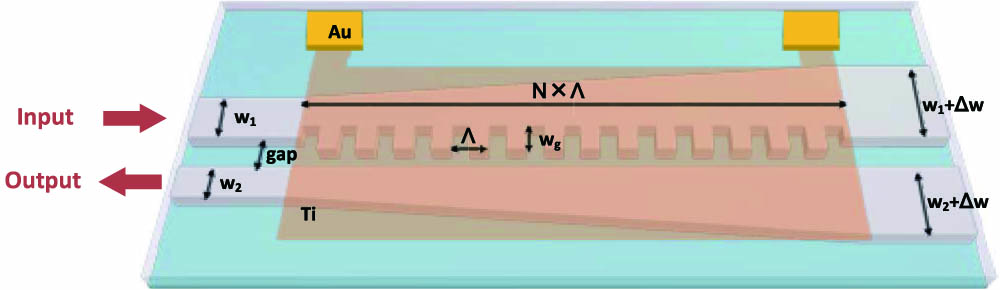
Figure 1.Scheme of the proposed integrated grating-assisted contradirectional couplers.
Since the Bragg gratings are not infinite in length, the Fourier transform of the gratings with rectangle function is typically a sinc function. This means the side-lobes and ripples will appear in the transmission spectrum. Fortunately, apodization technology has been developed and widely used in mature fiber gratings to suppress side-lobes and ripples. We simulate different apodization filters to achieve a flat-top response and ripple suppression. According to the analysis in Refs. [32,33] and tentative simulations, asymmetric cosine apodization is one of the most effective methods for ripple suppressions of transmission and group delay spectra. Thus, we adopt asymmetric cosine apodization; namely, the apodization function is only applied on the gratings near the input port. The ratio of apodization length to the whole grating length actually has an effect upon the transmission and group delay spectra, as shown in Fig. 2. The Bragg gratings are chosen with , , , , , and . Figure 2(a) shows that the ripples of the transmission spectra are reduced when asymmetric cosine apodization is applied. In addition, the bandwidth loss of 1/3 cosine apodization is lower than that of 1/2 cosine apodization. In Fig. 2(b), the ripples of group-delay spectra are well suppressed when asymmetric cosine apodization of either 1/3 or 1/2 cosine is applied. Ultimately, 1/3 cosine apodization is selected due to its superior performance.

Figure 2.(a) Simulated transmission spectra and (b) group-delay spectra for chirped Bragg gratings with different apodization filters applied. , , , , , .
The central wavelength of the Bragg gratings follows the Bragg equation, Here, and are determined by the device, so devices with various parameters are fabricated to investigate the effect on the transmission spectrum. The lengths of the fabricated devices are all about 1.8 mm, with . Figure 3(a) shows the measured transmission spectra for different chip samples. One can see that the transmission spectra are redshifted with increasing grating period, which agrees with the equation. In Fig. 3(b), the waveguide widths are designed as and . With wider waveguides, the effective index of the waveguide increases, which results in the redshifting of all the transmission spectra. In addition, the bandwidth of the wider waveguides is about 9 nm, which is smaller than that of the narrower waveguides. Next, chirp rate is varied by different of 10 nm and 20 nm. Figure 3(c) shows that large chirp rate results in a wider reflection bandwidth, i.e., 6.8 versus 12 nm. The measured results in Figs. 3(a)–3(c) are all based on unapodized gratings. In Fig. 3(d), unapodized and asymmetric apodized devices are compared, and it should be noted that the passband spectra of the gratings are smoother thanks to the apodization design.
Figure 3.(a) Measured transmission spectra of different grating periods with , , and . (b) Measured transmission spectra of different grating periods with and . (c) Measured transmission spectra of different with , , and . (d) Measured transmission spectra of unapodized and asymmetric apodized Bragg gratings with , , , and . (e) SEM image of apodized Bragg gratings. (d) SEM image of unapodized Bragg gratings.
The proposed structure is fabricated on a commercial SOI wafer which consists of a 250 nm silicon layer and a 3 μm buried oxide layer. First, the waveguide patterns are defined by electron beam lithography (EBL) on the commercial SOI wafer, and then the silicon is dry etched by the inductively coupled plasma etching process. Second, a 2 μm thick silicon dioxide layer is deposited using plasma-enhanced chemical vapor deposition (PECVD). Finally, the heaters are formed by depositing metal layers on the layer. Figures 3(e) and 3(f) show the scanning electron microscopy (SEM) micrographs of fabricated apodized and unapodized structures before PECVD deposition. It should be noted that the fabrication process requires high resolution of EBL to achieve slight amplitude modulation along the waveguide.
The tunability of time delay lines is achieved by the thermo-optic effect of the heating electrodes. A 100 nm thick titanium strip is deposited on top of the oxide cladding for thermal tuning, and 10 nm thick gold is deposited as conductive electrode. However, due to the millimeter-scale length of the Bragg gratings, the fabricated heating metal layer length is also millimeter-scale, with a large resistance. For example, the resistance of the strip heaters (type I) in Fig. 4(a) is measured as with a 1.71 μm wide, 1.8 mm long titanium strip. In this case, the spectrum drift is only 0.3 nm, and even the applied voltage is up to 20 V. To enhance the heating efficiency, heaters with parallel circuits (type II) are designed to reduce the resistance. The resistance of the type II heaters in Fig. 4(a) is measured as with a 3 μm wide, 100 nm thick, 1.8 mm long titanium strip. As shown in Fig. 4(b), type II heaters can achieve 4.68 nm spectrum drift when the applied voltage is 8 V. The heating efficiency is enhanced by about 94 times at 8 V voltage. The micrographs of the type I and type II devices are shown in Figs. 4(c) and 4(d), respectively. In this part, we propose a type II heater to improve heating efficiency for narrow and long waveguides. Of course, this is not the only way to reduce resistance; an alternative way is to increase the thickness and width of the heaters. However, the large width of the heaters will lead to a lower heating efficiency. Furthermore, increasing the thickness will be more expensive, and sometimes the thickness is limited by the standard process flow. The type II design offers the possibility of implementing a high-efficiency metal microheater by simply changing the design on the planar layer.
Figure 4.(a) Schematic of type I and type II heaters. (b) Spectral drift as a function of the applied voltage of the two types of heaters. Micrographs of (c) type I and (d) type II heaters.
3. RESULTS AND DISCUSSION
The experimental setup for the measurement of group delay is shown in Fig. 5. The optical carrier is provided by a tunable laser source (TLS) with optical power. Then the launched light passes through the polarization controller (PC1) and 10 GHz intensity modulator (IM). The 10 GHz radio frequency (RF) signal is loaded on the IM through the RF amplifier. Afterwards, a 10 GHz modulated sinusoidal signal is created. The signal is then injected into the proposed device via PC2, and is finally detected by an oscilloscope (OSC). The PCs are used to maximize the efficiency of mode coupling. The two erbium-doped fiber amplifiers are used to compensate link loss, and the attenuator is used to protect the OSC. The fiber-to-fiber insertion loss is about 6 dB. When the input wavelength changes within the passband, the detected waveforms will have different time delays. By comparing the time delay at different wavelengths, the group delay lines can be calculated.
Figure 5.Experimental setup of the time-delay measurement. TLS, tunable laser source; PC, polarization controller; RF, radio frequency; IM, intensity modulator; EDFA, erbium-doped fiber amplifier; ATT, attenuator; OSC, oscilloscope.
There are two modes for delay tuning using optical delay lines. One mode is to tune the time delay by changing the optical carrier wavelength. However, this tuning mode relies on a laser source with a tunable wavelength. In most cases, the laser source has a fixed wavelength without tunability. Another mode is to tune the time delay by the drift of dispersion curve driven by the loaded voltage. In this case, the laser source does not need to tune its wavelength. To prevent the breakdown of the metal microheater, the driving voltage is limited to less than 8 V, thus restraining the maximum delay tuning range. This can be further improved by optimizing electrode thickness and resistance characteristics. In the measurement that follows, the two cases both will be discussed.
Figure 6 shows the measured spectral responses and group delay lines of unapodized and asymmetric apodized fabricated devices of 1.8 mm length. In the absence of voltage, the passband of the unapodized device in Fig. 6(a) is 12 nm. The insertion loss near the band edge at the short-wavelength side (1541.4 nm) and long-wavelength side (1552 nm) are 0.5 and 2.7 dB, respectively. In Fig. 6(b), the passband of the apodized device is 8 nm. The insertion loss near the band edge at the short-wavelength side (1536.5 nm) and long-wavelength side (1544.2 nm) are 1.33 and 2.6 dB, respectively. It can be seen that the passband of the apodized device is smoother than that of the unapodized one, and both spectra can maintain the same shape under different voltages of 0, 5.2, and 7.2 V. We also notice that the apodization method brings ripple suppression at the cost of bandwidth reduction and delay loss. In Fig. 6(c), the total time delay of the unapodized device in the passband is about 55 ps, and when the device is operating at heating status, the group delay lines have large fluctuations. In Fig. 6(d), the total delay of the apodized device is reduced to 50 ps, but both the linearity and consistency have been improved. A figure of merit to evaluate the delay line performance is the loss per ns delay increment (in dB/ns unit). This parameter is 40 and 25.4 dB/ns for the unapodized and apodized device, respectively. Compared to the parameter in Refs. [30] (9.6 dB/ns) and [31] (21 dB/ns), the device loss can be further reduced by waveguide mode optimization. In conclusion, the apodization method can improve the performance of Bragg gratings in terms of spectral flatness, delay line linearity, and optical loss.
Figure 6.Measured spectral responses of (a) unapodized and (b) asymmetric apodized fabricated devices. Measured group delay lines of (c) unapodized and (d) asymmetric apodized fabricated devices.
When the laser wavelength is scanned within the passband of the gratings, the output optical signals will have different delay values. To demonstrate the delay tunability, we measured the output waveforms with different wavelengths after propagating in the apodized device, as shown in Fig. 7. The gray dot curves and red curves in Fig. 7 represent the 10 GHz input sine waveforms and delayed waveforms, respectively. By changing the optical carrier wavelength from 1535 to 1545 nm, the delay tuning range is about 50 ps. In addition, there is no distortion in the output waveforms at a modulated bandwidth of 10 GHz. Under thermal tuning mode, the actual delay tuning range for the devices is around 20 ps at 7.2 V.
Figure 7.10 GHz optical waveforms with different wavelengths after passing through the apodized device. Gray dot curves represent input waveforms; red curves represent delayed waveforms.
For the schemes based on chirped Bragg gratings, the maximum group delay is limited by the grating length. To improve the group delay of a certain length, we propose a method to combine the scheme with an ultra-compact reflector [34] for doubling group delay, as shown in Fig. 8(a). The reflector is set at the original output port of the contradirectional couplers, so the light of different wavelengths can return to the input port through different paths. A Y-branch is introduced at the input port, so it introduces an extra loss of about 6 dB. This method improves the utilization of the Bragg gratings. It should be noted that the use of a reflector can obtain a doubled delay amount, but an insertion loss of about 6 dB is introduced by the Y-branch at the input port. The use of a Y-branch is convenient for measurement, and it can be removed in the practical application. Despite the Y-branch, the insertion losses are almost the same compared to a grating of double length, and the proposed device has more compact size. In the future, we can reduce the chip size with a spiral pattern design [35,36].
Figure 8.(a) Schematic of a novel structure combining the grating-assisted contradirectional couplers with an ultra-compact reflector. (b) Measured spectral responses and (c) group delay lines of the fabricated device at different voltages. (d) Micrograph of the fabricated device.
The micrograph of the fabricated device with 6 mm long Bragg gratings is shown in Fig. 8(d). The reflector has a compact size of , which has almost no impact on the overall device size. The resistance of type II heaters in Fig. 8(d) is measured as with a 3 μm wide, 200 nm thick, 6 mm long titanium strip. The measured spectral responses and group delay lines of the fabricated device are shown in Figs. 8(b) and 8(c). In Fig. 8(b), the passband of the device is 12 nm. The insertion loss near the band edge at the short-wavelength side (1536.5 nm) and long-wavelength side (1549 nm) are 7 and 15 dB, respectively. In the group delay measurement, a 5 GHz modulated sinusoidal signal is employed as the test signal. In Fig. 8(c), the measured group delay can achieve 400 ps within the passband of 12 nm. The delay lines have a slope of 33 ps/nm, indicating a positive chromatic dispersion of , which is enhanced by times compared to the dispersion of single-mode fiber with 17 ps/(nm·km) dispersion. Compared to recent research about dispersion engineering, our chip design may pave the way for on-chip large-dispersion units with a compact size [37–39]. With increasing applied voltage, a redshift occurs in both the spectral responses and group delay lines. However, due to the reflection between the Y-branch and reflector, there are some ripples in the transmission spectra, and the transmission has a larger attenuation at the longer wavelength. When the applied voltage is up to 8 V, distortion occurs in the group delay lines. Due to the long waveguide length, the waveguide and heater distribution cannot be completely uniform in the propagation direction. Since the waveguide is heated unevenly, the transmission spectrum resonates at some wavelengths, resulting in a sudden change in phase, so the delay at some wavelengths fluctuates. Further optimizations are required to avoid resonance among the device.
Due to the large group delay fluctuations and dispersion of the grating-assisted contradirectional couplers with an ultra-compact reflector, we use a narrow-bandwidth optical signal of 5 GHz to evaluate the performance of the device. The gray dot curves and red curves in Fig. 9 represent the 5 GHz input sine waveforms and delayed waveforms, respectively. With the input wavelength increasing from 1536 to 1550 nm, 400 ps delay tuning range can be achieved. We can see that the delayed waveform at 1540 nm has slight distortion, which is caused by the group delay fluctuations. In general, the output waveform can maintain sine waveform within the passband.
Figure 9.5 GHz optical waveforms with different wavelengths after passing through the gratings with an ultra-compact reflector. Gray dot curves represent input waveforms; red curves represent delayed waveforms.
4. CONCLUSION
To summarize, we propose and demonstrate tunable optical delay lines based on integrated grating-assisted contradirectional couplers. We studied and optimized device performance from several aspects, including parameter optimization, apodization analysis, and electrode and large delay design. Finally, tunable group delay lines of 50 ps at different wavelengths within the bandwidth of 12 nm are realized with an apodized Bragg grating length of 1.8 mm. The delay tuning range under thermal tuning mode is about 20 ps, and it maintains good linearity and consistency at different voltages. In addition, a novel structure combining the grating-assisted contradirectional couplers with an ultra-compact reflector is discussed and a large group delay of 400 ps within the bandwidth of 12 nm is achieved. The delay tuning range under the thermal tuning mode is about 100 ps. A dispersion value up to with bandwidth of 12 nm is demonstrated in the communication band. Our work paves the way for on-chip tunable delay lines and large-dispersion devices.
References
[1] F. Xia, L. Sekaric, Y. Vlasov. Ultracompact optical buffers on a silicon chip. Nat. Photonics, 1, 65-71(2007).
[2] M. Moralis-Pegios, N. Terzenidis, G. Mourgias-Alexandris, K. Vyrsokinos, N. Pleros. A low-latency high-port count optical switch with optical delay line buffering for disaggregated data centers. Proc. SPIE, 10538, 1053805(2018).
[3] J. L. Corral, J. Marti, J. M. Fuster, R. I. Laming. True time-delay scheme for feeding optically controlled phased-array antennas using chirped-fiber gratings. IEEE Photon. Technol. Lett., 9, 1529-1531(1997).
[4] C. R. Doerr, S. Chandrasekhar, P. J. Winzer, A. R. Chraplyvy, A. H. Gnauck, L. W. Stulz, R. Pafchek, E. Burrows. Simple multichannel optical equalizer mitigating intersymbol interference for 40-Gb/s nonreturn-to-zero signals. J. Lightwave Technol., 22, 249-256(2004).
[5] F. Wang, X. Zhang. Photonic generation of ultrawideband signals using a delay interferometer. Front. Optoelectron. China, 3, 179-183(2010).
[6] Z. Hu, J. Xu, M. Hou. Theoretical demonstration of all-optical switchable and tunable UWB doublet pulse train generator utilizing SOA wavelength conversion and tunable time delay. Front. Optoelectron., 10, 180-188(2017).
[7] R. L. Moreira, J. Garcia, W. Li, J. Bauters, J. S. Barton, M. J. R. Heck, J. E. Bowers, D. J. Blumenthal. Integrated ultra-low-loss 4-bit tunable delay for broadband phased array antenna applications. IEEE Photon. Technol. Lett., 25, 1165-1168(2013).
[8] V. C. Duarte, J. G. Prata, C. Ribeiro, R. N. Nogueira, G. Winzer, L. Zimmermann, R. Walker, S. Clements, M. Filipowicz, M. Napierała, T. Nasiłowski, J. Crabb, L. Stampoulidis, J. Anzalchi, M. V. Drummond. Integrated photonic true-time delay beamformer for a Ka-band phased array antenna receiver. Optical Fiber Communication Conference, M2G.5(2018).
[9] H. Lee, T. Chen, J. Li, O. Painter, K. J. Vahala. Ultra-low-loss optical delay line on a silicon chip. Nat. Commun., 3, 867(2012).
[10] X. Wang, B. Howley, M. Y. Chen, R. T. Chen. Phase error corrected 4-bit true time delay module using a cascaded 2 × 2 polymer waveguide switch array. Appl. Opt., 46, 379-383(2007).
[11] J. Xie, L. Zhou, Z. Li, J. Wang, J. Chen. Seven-bit reconfigurable optical true time delay line based on silicon integration. Opt. Express, 22, 22707-22715(2014).
[12] X. Wang, L. Zhou, R. Li, J. Xie, L. Lu, K. Wu, J. Chen. Continuously tunable ultra-thin silicon waveguide optical delay line. Optica, 4, 507-515(2017).
[13] D. Perez, E. S. Gomariz, J. Capmany. Programmable true-time delay lines using integrated waveguide meshes. J. Lightwave Technol., PP, 1(2018).
[14] R. Kashyap, M. de Lacerda Rocha. On the group delay characteristics of chirped fibre Bragg gratings. Opt. Commun., 153, 19-22(1998).
[15] G. Lenz, B. J. Eggleton, C. K. Madsen, R. E. Slusher. Optical delay lines based on optical filters. IEEE J. Quantum Electron., 37, 525-532(2001).
[16] L. Y. Mario, M. K. Chin. Optical buffer with higher delay-bandwidth product in a two-ring system. Opt. Express, 16, 1796-1807(2008).
[17] M. S. Rasras, C. K. Madsen, M. A. Cappuzzo, E. Chen, L. T. Gomez, E. J. Laskowski, A. Griffin, A. Wong-Foy, A. Gasparyan, A. Kasper, J. L. Grange, S. S. Patel. Integrated resonance-enhanced variable optical delay lines. IEEE Photon. Technol. Lett., 17, 834-836(2005).
[18] F. Morichetti, A. Melloni, A. Breda, A. Canciamilla, C. Ferrari, M. Martinelli. A reconfigurable architecture for continuously variable optical slow-wave delay lines. Opt. Express, 15, 17273-17282(2007).
[19] A. Melloni, F. Morichetti, C. Ferrari, M. Martinelli. Continuously tunable 1 byte delay in coupled-resonator optical waveguides. Opt. Lett., 33, 2389-2391(2008).
[20] F. Morichetti, A. Melloni, C. Ferrari, M. Martinelli. Error-free continuously-tunable delay at 10 Gbit/s in a reconfigurable on-chip delay-line. Opt. Express, 16, 8395-8405(2008).
[21] J. Xie, L. Zhou, Z. Zou, J. Wang, X. Li, J. Chen. Continuously tunable reflective-type optical delay lines using microring resonators. Opt. Express, 22, 817-823(2014).
[22] C. Xiang, M. L. Davenport, J. B. Khurgin, P. A. Morton, J. E. Bowers. Low-loss continuously tunable optical true time delay based on Si3N4 ring resonators. IEEE J. Sel. Top. Quantum Electron., 24, 1-9(2018).
[23] J. Li, T. P. White, L. O’Faolain, A. Gomez-Iglesias, T. F. Krauss. Systematic design of flat band slow light in photonic crystal waveguides. Opt. Express, 16, 6227-6232(2008).
[24] J. Adachi, N. Ishikura, H. Sasaki, T. Baba. Wide range tuning of slow light pulse in SOI photonic crystal coupled waveguide via folded chirping. IEEE J. Sel. Top. Quantum Electron., 16, 192-199(2010).
[25] A. Melloni, A. Canciamilla, C. Ferrari, F. Morichetti, L. O. Faolain, T. F. Krauss, R. D. L. Rue, A. Samarelli, M. Sorel. Tunable delay lines in silicon photonics: coupled resonators and photonic crystals, a comparison. IEEE Photon. J., 2, 181-194(2010).
[26] C.-Y. Lin, H. Subbaraman, A. Hosseini, A. X. Wang, L. Zhu, R. T. Chen. Silicon nanomembrane based photonic crystal waveguide array for wavelength-tunable true-time-delay lines. Appl. Phys. Lett., 101, 051101(2012).
[27] C.-J. Chung, X. Xu, G. Wang, Z. Pan, R. T. Chen. On-chip optical true time delay lines featuring one-dimensional fishbone photonic crystal waveguide. Appl. Phys. Lett., 112, 071104(2018).
[28] S. Khan, M. A. Baghban, S. Fathpour. Electronically tunable silicon photonic delay lines. Opt. Express, 19, 11780-11785(2011).
[29] G. Brunetti, D. Conteduca, F. Dell’Olio, C. Ciminelli, M. N. Armenise. Design of an ultra-compact graphene-based integrated microphotonic tunable delay line. Opt. Express, 26, 4593-4604(2018).
[30] I. Giuntoni, D. Stolarek, D. I. Kroushkov, J. Bruns, L. Zimmermann, B. Tillack, K. Petermann. Continuously tunable delay line based on SOI tapered Bragg gratings. Opt. Express, 20, 11241-11246(2012).
[31] W. Shi, V. Veerasubramanian, D. Patel, D. V. Plant. Tunable nanophotonic delay lines using linearly chirped contradirectional couplers with uniform Bragg gratings. Opt. Lett., 39, 701-703(2014).
[32] D. Tan, K. Ikeda, R. Saperstein, B. Slutsky, Y. Fainman. Chip-scale dispersion engineering using chirped vertical gratings. Opt. Lett., 33, 3013-3015(2008).
[33] R. Kashyap. Fiber Bragg Gratings(1999).
[34] Y. Wang, S. Gao, K. Wang, H. Li, E. Skafidas. Ultra-broadband, compact, and high-reflectivity circular Bragg grating mirror based on 220 nm silicon-on-insulator platform. Opt. Express, 25, 6653-6663(2017).
[35] Z. Chen, J. Flueckiger, X. Wang, F. Zhang, H. Yun, Z. Lu, M. Caverley, Y. Wang, N. A. Jaeger, L. Chrostowski. Spiral Bragg grating waveguides for TM mode silicon photonics. Opt. Express, 23, 25295-25307(2015).
[36] Z. Zou, L. Zhou, M. Wang, K. Wu, J. Chen. Tunable spiral Bragg gratings in 60-nm-thick silicon-on-insulator strip waveguides. Opt. Express, 24, 12831-12839(2016).
[37] D. T. H. Tan, K. Ikeda, R. E. Saperstein, B. Slutsky, Y. Fainman. Chip-scale dispersion engineering using chirped vertical gratings. Opt. Lett., 33, 3013-3015(2008).
[38] E. Sahin, K. J. A. Ooi, C. E. Png, D. T. H. Tan. Large on-chip dispersion using cladding-modulated 1D photonic crystals. Opto-Electronics and Communications Conference (OECC) and Photonics Global Conference (PGC), 1-3(2017).
[39] E. Sahin, K. J. A. Ooi, C. E. Png, D. T. H. Tan. Large, scalable dispersion engineering using cladding-modulated Bragg gratings on a silicon chip. Appl. Phys. Lett., 110, 161113(2017).


