1Research Center for Optical Fiber Sensing, Zhejiang Laboratory, Hangzhou 311100, China
2Research Center for Intelligent Optoelectronic Computing, Zhejiang Laboratory, Hangzhou 311100, China
3International Research Center for Advanced Photonics, College of Optical Science and Engineering, Zhejiang University, Hangzhou 310058, China
4Fiber Optics Research Center (FORC), Key Laboratory of Optical Fiber Sensing and Communications, University of Electronic Science and Technology of China, Chengdu 611731, China
【AIGC One Sentence Reading】:We achieved ultra-high extinction ratio optical pulse modulation using a thin film lithium niobate modulator, enhancing distributed acoustic sensing performance with improved sensitivity and crosstalk suppression.
【AIGC Short Abstract】:We achieved ultra-high extinction ratio optical pulse modulation using a thin film lithium niobate electro-optical modulator. By cancelling the relaxation-tail response, an extinction ratio exceeding 50 dB was reached. This enhanced modulation was applied in distributed acoustic sensing, boosting sensitivity and spatial crosstalk suppression, thus significantly improving sensing performance.
Note: This section is automatically generated by AI . The website and platform operators shall not be liable for any commercial or legal consequences arising from your use of AI generated content on this website. Please be aware of this.
Abstract
We experimentally demonstrate ultra-high extinction ratio (ER) optical pulse modulation with an electro-optical modulator (EOM) on thin film lithium niobate (TFLN) and its application for fiber optic distributed acoustic sensing (DAS). An interface carrier effect leading to a relaxation-tail response of TFLN EOM is discovered, which can be well addressed by a small compensation component following the main driving signal. An ultra-high ER > 50 dB is achieved by canceling out the tailed response during pulse modulation using the EOM based on a cascaded Mach–Zehnder interferometer (MZI) structure. The modulated optical pulses are then utilized as a probe light for a DAS system, showing a sensitivity up to (7 pε/√Hz) for 2-km single-mode sensing fiber. Spatial crosstalk suppression of 24.9 dB along the fiber is also obtained when the ER is improved from 20 dB to 50 dB, clearly revealing its importance to the sensing performance.
1. INTRODUCTION
Ultra-high extinction ratio (ER) optical modulation is of great importance for a variety of applications such as quantum key distribution [1,2], lidar [3,4], and distributed optical fiber sensing (DOFS) [5–9]. The signal-to-noise ratios or crosstalk in these systems are contributed considerably by the leakage light at the “off” states during modulation [2,10]. For example, when optical pulses are launched into the sensing fiber of a phase-sensitive optical time domain reflectometry (-OTDR) system, the non-zero continuous wave (CW) light between pulses interacts with the fiber all the time and produces crosstalk along the whole fiber. Conventionally, ultra-high ER () modulations are implemented by acousto-optical modulators (AOMs), which are widely employed in the applications abovementioned. However, the bulky nature and power consumption () of discrete AOM devices have hindered further improvement of system compactness and power efficiency, not to mention their modulation bandwidth () limited by the response time of acousto-optical crystals [11].
Recently, the successful micro/nano processing of thin film lithium niobate (TFLN) has realized various high-performance photonic devices on this platform for optical communication [12,13], optical signal processing [14,15], and novel fundamental researches [16–18]. Particularly, benefiting from the advantages of high efficiency ( [19]), high bandwidth ( [20,21]), linear phase modulation [22], etc., electro-optical modulators (EOMs) based on TFLN are developing rapidly and are ready for commercialization. The on-chip integrated EOMs are promising for miniatured opto-electronic modules/systems that require small device footprints, high levels of integration, and low power consumption. Mach–Zehnder interferometers (MZIs) are the most utilized structure for optical intensity modulation on TFLN [23]. Unfortunately, owing to fabrication errors, the balance of the two interference arms of an MZI is usually far from being perfect, leading to a limited ER less than 30 dB. To address the imbalance issue, cascaded MZI structure has been proposed [24], in which extra MZIs are added to finely tune the power ratio of the two arms in the modulation MZI. About 40-dB and 50-dB ERs were experimentally demonstrated using this structure on TFLN according to the given static transmission contrast in Refs. [25,26], respectively. With the same configuration, the other reports based on a silicon-on-insulator (SOI) platform also presented similar static results [27,28]. However, a direct demonstration of dynamic modulation with an ultra-high ER using a TFLN EOM is still absent. Whether the electro-optical (EO) response of the on-chip EOM in near-perfect interference can completely follow pulsed electrical driving and maintain the high ER obtained in static characterization is also in doubt.
In this work, a cascaded-MZI EOM on TFLN and generation of optical pulses with an ER up to 51 dB are experimentally demonstrated. The ultra-high dynamic ER modulation is verified by a self-heterodyne measurement instead of an oscilloscope with rather limited dynamic range. Micro heaters are used in the first MZI to stably tune the balancing of the modulation MZI. A relaxation tail is observed in the EO response when nano-second pulsed electrical driving is applied to the EOM. The slowing-down decay on the falling edge of a modulated optical pulse appears after the intensity decreases instantaneously from peak by more than 20 dB. As a result, the optical pulses are broadened from the bottom by a few micro-seconds, which severely influences the quality of high-ER pulses. Through comprehensive investigation, charge carriers at the interface between the different dielectric materials are discovered to be responsible for such a relaxation phenomenon. Due to the pronounced interface conductivity, an internal electric field is formed upon external driving and lasts for a certain amount of time when the external potential is removed. Therefore, the TFLN phase shifters are still being modulated by the residual field until its complete decay. This theory is verified by our experiment and numerical simulation. We thus append a compensation component right after the square pulse driving signal and successfully cancel out the relaxation tail in the modulated optical pulses from the TFLN EOM. Furthermore, The EOM is employed in a distributed acoustic sensing (DAS) system for generating ultra-high ER pulses with a CW laser input. The modulation power consumption is estimated to be less than 16.8 mW, much less than that of a typical AOM. Impacts of ER and relaxation tail of the probe pulses on the DAS performances are studied in detail. As a result, 24.9-dB crosstalk reduction is obtained by 30-dB ER enhancement. The relaxation tail is also found to be influencing the crosstalk remarkably, which is dependent on the pulse repetition rate. Eventually, a high sensitivity of (ε) at 500 Hz–5 kHz for 2-km single-mode sensing fiber is achieved, revealing the application potential of on-chip TFLN EOM for compact and low-power sensing systems. Meanwhile, the discovery of the interface conductivity effect in the popular configuration may provide valuable insight for novel device designs and fundamental scientific explorations.
Sign up for Photonics Research TOC. Get the latest issue of Photonics Research delivered right to you!Sign up now
2. DEVICE DESIGN, FABRICATION, AND CHARACTERIZATION
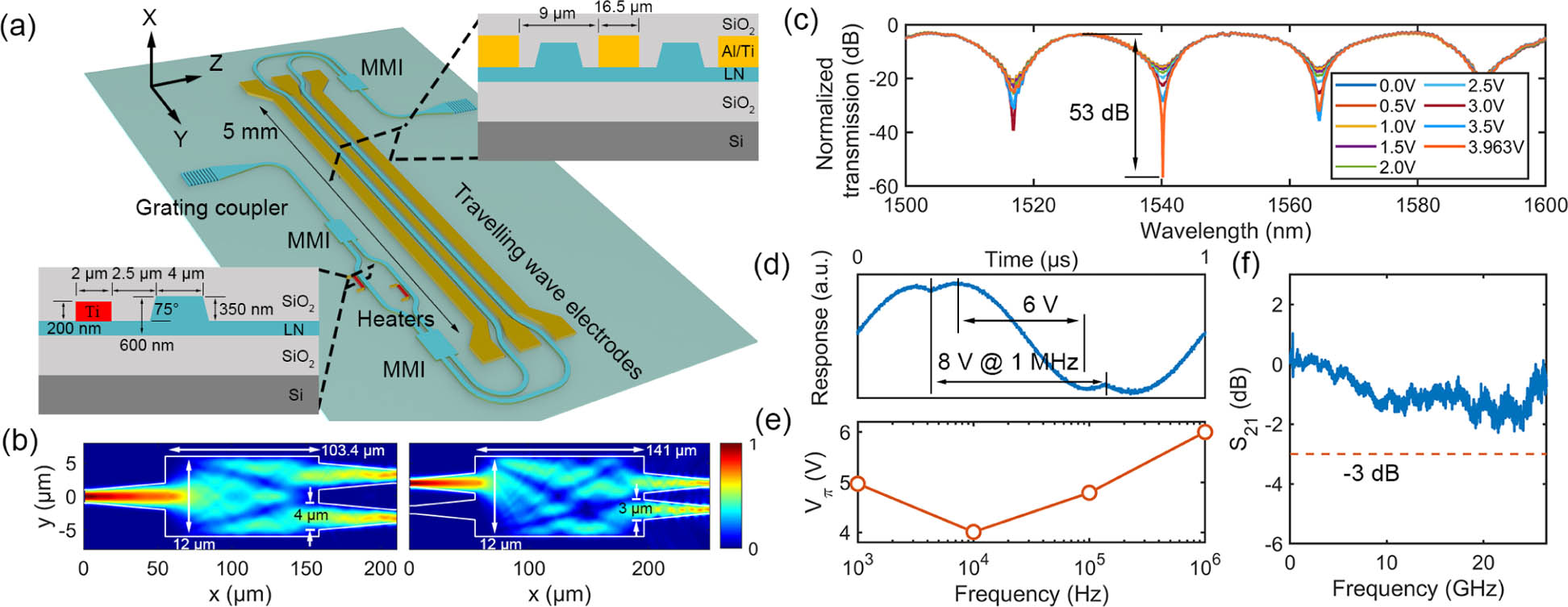
The schematic of the cascaded-MZI EOM on an X-cut TFLN substrate is shown in Fig. 1(a). The 600-nm lithium niobate (LN) layer is on 3-μm-thick buried silicon oxide. In the cascaded MZI structure, the former MZI has two Ti micro heaters near both its arms. By applying DC voltage to the heaters and thus changing the refractive index of the heated TFLN waveguides, the power ratio of the two outputs from the multimode interferometer (MMI) can be finely tuned. As the MMI outputs are also inputs of the latter modulation MZI, perfect balance can be achieved in principle. EO tuning is not adopted at the first stage due to the instability induced by DC drift of LN [13,29,30], which would gradually shift the balanced state away over time. In contrast, thermo-optic tuning has been demonstrated with much better stability [30]. Its slow response is also not a concern as the tuning voltage will hold once optimized. The length, width, and height of the Ti heaters are 200 μm, 2 μm, and 200 nm, respectively, while the separation between the heaters and the waveguides is 2.5 μm. The latter modulation MZI consists of a pair of 5-mm-long phase shifter arms along the Y axis and corresponding traveling wave electrodes in a ground–signal–ground (GSG) configuration. EO modulation based on the Pockels effect of TFLN is adopted here for high-speed response. The widths of the ground and signal tracks are 80 μm and 16.5 μm, respectively, while the distance between them is 9 μm. A MMI is used inversely as a combiner after the phase shifters. All the MMIs are designed with 3-dB splitting ratio around 1550-nm wavelength. Their structural parameters and corresponding simulated electric field magnitude distributions are given in Fig. 1(b). The calculated transmission efficiencies of a single output port are 49.9% for the MMI and 48.7% for the MMI at 1550 nm. In order to reduce insertion loss of the millimeter-long phase shifters, the waveguide width is adiabatically increased from 1.2 μm to 4 μm before entering the phase shifter section. Grating couplers are employed as EOM input and output ports.
Figure 1.(a) Schematic of the cascaded-MZI EOM. Insets: cross-section views of the thermo-optic structure in the first MZI and the electro-optical structure in the second (modulation) MZI. (b) Electric field magnitude distributions of the MMI (left) and MMI (right) used in the modulator. (c) Measured transmission spectra for different DC voltages applied to the heater. (d) EO response under triangular-wave driving at 1-MHz frequency. (e) Measured versus driving frequency. (f) Measured EO bandwidth () of the EOM.
To fabricate the EOM devices, an X-cut TFLN substrate is patterned by electron beam lithography (EBL) with hard masks ( and Cr) on top. Note that soft masks such as hydrogen silsesquioxane (HSQ) are also popular in EBL processes on TFLN. Then, the LN layer is etched by 350 nm using inductively coupled plasma reactive ion etching (ICP RIE) to form the rib waveguide structures. Subsequently, the Ti heaters and Al traveling wave electrodes are deposited and patterned on the 250-nm TFLN slab; 10-nm Ti is also deposited right before the Al electrodes for enough adhesion. Finally, the device chip is cladded by 1.5-μm-thick with electrode openings for probing or wire-bonding. Due to the fabrication error induced by UV photolithography, the gap size between the traveling wave electrodes turns out to be about 8 μm according to microscopy characterization.
The static transmission of the fabricated EOM on TFLN is measured with a tunable laser (Santec TSL-710) and a synchronized optical power meter (Santec MPM-210). DC voltage is also applied to one of the heaters in the first MZI to examine ER change. Because the TFLN phase shifters are designed to be working with TE mode, a fiber polarization controller (PC) is employed to control the EOM input polarization. A polarization extinction ratio over 42 dB can be obtained by adjusting the PC. The light is first coupled into a reference waveguide with two TE grating couplers. The measured peak efficiency of the grating coupler is about at 1560 nm and the 3-dB working bandwidth is about 54 nm, under a fiber tilting angle of 9°. The PC adjustment for polarization optimization is done when the waveguide transmitted power is maximized. Then, the TE light is coupled into the EOM via its own input grating. As shown in Fig. 1(c), the transmission normalized to the reference waveguide presents a typical interference spectrum, in which the ER around 1540-nm wavelength gradually increases with the applied voltage. This result indicates an effective power ratio adjustment of the MZI outputs via the thermo-optic effect. Initially less than 20 dB, the ER is improved to 53 dB at about 4-V DC bias. The on-chip insertion loss is about 2.7 dB, mainly owing to the sidewall roughness of TFLN waveguides. Outside the 3-dB bandwidth of the grating couplers, the modulator transmission can still be normalized correctly as long as the detected light is transmitted through the gratings instead of other paths, e.g., scattering. Next, a triangular driving signal is applied to the second (modulation) MZI in a push–pull configuration to measure of the EOM. From the optical output with a partial sinusoidal waveform in 1-MHz repetition [Fig. 1(d)], of 6 V is obtained according to the temporal separation between the maximum and minimum of the waveform. We also find that is dependent on the repetition frequency [Fig. 1(e)], which will be explained later. Besides, the modulation efficiency can be further improved with optimized phase shifter designs (Appendix A). Then, the EO bandwidth of the EOM is characterized with a high-speed photodetector (Newport 1474-A) and a vector network analyzer (Keysight E5080B). Two RF probes (GGB 40A) are used for EOM driving and signal termination. The obtained frequency response given in Fig. 1(f) shows that the 3-dB bandwidth is over 26 GHz, while measurement of the actual bandwidth is limited by the available frequency range of the vector network analyzer.
The conventional method using a photodetector (PD) and an oscilloscope for optical waveform observation is not able to measure an ER over 30 dB due to the limited dynamic range of oscilloscopes. To study the dynamics of ultra-high ER modulation with the TFLN EOM, we utilize a self-heterodyne setup [Fig. 2(a)] to measure the beat signal of the interference between the modulated light and a CW reference light. In this setup, the laser output is split into two paths. One is passed through the EOM and subsequently passed through an acousto-optic frequency shifter (200 MHz), while the other one acts as the constant reference. The interference light is then collected by a PD and analyzed by an electrical spectrum analyzer (ESA) with a large dynamic range (). As the beat signal power is proportional to the optical power of either path (Appendix B), one can use the zero-span mode of the ESA (Rohde & Schwarz FSW26) to inspect the beat signal at 200 MHz and thus obtain the temporal dynamics of the modulated light with an ultra-high ER. Note that a polarizer is employed after the EOM output to suppress unwanted optical polarization. Although only mode is coupled into the EOM, mode can also be excited in the EOM circuit possibly. For example, slight fiber-grating misalignment (Appendix D) or non-adiabatic transmission in waveguide bends [31] can excite mode, which would be easily hybridized with mode in taper waveguides accessing to the grating couplers [32]. Hence, the unwanted polarization needs to be blocked to prevent the interference from the light that is not being modulated correctly.
Figure 2.(a) Schematic of the self-heterodyne measurement setup. AWG, arbitrary waveform generator; PC, polarization controller; AOFS, acousto-optic frequency shifter; PD, photodetector; ESA, electrical spectrum analyzer. Inset: micrograph of the TFLN EOM. (b) Measured high-ER waveform of modulated optical pulse train. (c) Zoom-in waveform of the red dashed box in (b).
The TFLN EOM is then driven by a pulsed signal to modulate CW input into optical pulses. To realize high-ER modulation, proper DC voltage is applied to the first MZI and the wavelength is set at near-perfect destructive interference. The pulse duration is set as 200 ns considering the limited resolution bandwidth (10 MHz) of the ESA. A small duty cycle of 0.2% (i.e., 10-kHz repetition) is adopted to make the EOM recover from the driven state as much as possible. Therefore, the driving signal is mostly at 0 V except for the short appearance of electrical pulse peaks at about 5.8 V. Such a kind of driving scheme (ns-duration and repetition) is also frequently used for high-ER optical pulse generation in DOFS where the on-chip TFLN EOM could find an application opportunity. By finely tuning the voltage applied to the heater in the first MZI, we obtain the modulated pulse waveform (normalized to the pulse peak) with a power contrast up to 55 dB near the onsets of pulses, as shown in Fig. 2(b). However, a significant relaxation tail is also observed from the pulse response [Fig. 2(c)]. The slow decay in μs-scale occurs when the pulse signal drops by about 20 dB at voltage-off and thus would not be seen in low-ER modulation. As the decaying signal touches the noise floor, it rises slightly until the arrival of the next driving pulse. With the strong leakage light, these modulated optical pulses from the TFLN EOM are unfortunately not ideal for practical applications.
The observed relaxation phenomenon is found to be highly associated with the interface conductivities between adjacent layers of different materials in the TFLN waveguide structure. The conductivities of the upper--TFLN and the lower--Si interfaces are verified by DC measurements on the GSG electrodes and another unpatterned TFLN substrate, respectively. Figure 3(a) gives the measured current against voltage for the two interfaces and their probing methods. The deduced surface conductivities are and for the first and third interfaces, respectively. For the latter one, similar conductivity is observed on an SOI substrate as well, where the charges induced by structural defects form a parasitic-surface–conduction interface between the handle layer and buried oxide [33,34]. However, the conductivity of the interface between TFLN and lower- is difficult to measure directly. Therefore, we build a simulation model [Fig. 3(b)] to fit the measured step response of the EOM by adjusting the conductivity of the second interface. In this way, this parameter can be reasonably determined.
Figure 3.(a) Measured current versus voltage for the upper--TFLN and the lower- -Si interfaces using the probing methods on the left. (b) Proposed electrical model with three interface conductivities. (c) Experimental step response of the EOM and simulated responses with , , and . (d) Simulated temporal evolutions of horizontal electric field at waveguide center [red triangle marked in (b)] driven by pulses of 200-ns, 400-ns, and 600-ns durations. (e) Simulated electric field distributions at the moments I–IV marked in (d). (f) Experimental and simulated EOM response driven by pulses of 200-ns, 400-ns and 600-ns durations.
The electric field simulation is performed by COMSOL, and the effective refractive index change of waveguide mode is calculated by Lumerical Mode. A previous study suggested that the thickness of the conducting interface layer is down to about 2 nm [35]. Here, we use three 10-nm layers to represent the interfaces for a tradeoff between simulation precision and computation load, which gives very similar results compared with that of a test simulation with thinner layers. All the material parameters for the electrical simulation are summarized in Table 1. Note that the average of dielectric constants of two adjacent materials is used to represent the dielectric property of an interface layer. Actually, these parameters have very little effect. Because the response is RC dominated and the capacitance is proportional to the dielectric constant, the interface layers are too thin to produce a noticeable capacitive effect when they are in serial connection with the tiny capacitors formed by the other μm-thick layers. This is verified by repeating the simulation using different interface dielectric constants. With the calculated electric field distributions, the field-induced anisotropic permittivity perturbation to a TFLN waveguide can be obtained using the relation [36] where are the parameters of the Pockels tensor. The values of , , , in Voigt notation are taken as 9.6, 6.8, 30.9, and 32.6 pm/V [37], respectively. Then, the transient optical mode index and corresponding phase shift can be deduced. In experiment, the step response of the phase [solid line in Fig. 3(c)] is obtained by driving the EOM with a 1-Hz square wave signal. The instantaneous phase change at voltage-on is followed by a slow variation, whose trend is strongly dependent on [dashed line in Fig. 3(c)] according to the simulation. As a result, the experiment response is well fitted with .
Electric Parameters Used in Simulation
Material
LN
Silicon
Silica
Air
Al
Interface 1
Interface 2
Interface 3
Relative dielectric constant
[86,86,29]
11.9
4
1
1
45
45
8
Conductivity (S/m)
820
With all the interface conductivities, the relaxation-tail response of the TFLN EOM under pulsed driving can be reproduced numerically. Temporal evolutions of the horizontal electric field intensity at the waveguide center [red triangle in Fig. 3(b)] driven by unit-volt potential are calculated and depicted in Fig. 3(d). The pulsed driving signal is switched on at 0 ns and lasts for a few hundred ns (200, 400, and 600 ns). Upon voltage-off and substantial field intensity decrease, a weak residual field appears with an exponential-like decay for a few μs. Such a residual field directly influences the EOM output intensity via the Pockels effect of the TFLN and hence leads to the relaxation tail during pulse modulation. Two-dimensional electric field distributions around the TFLN waveguide are also simulated and displayed for three stages of the temporal response as shown in Fig. 3(e). Stages I and II represent the external driving effect and relaxation tail, respectively, while Stage III shows a reversed field distribution near the waveguide. Additionally, longer external driving brings a stronger residual field, which can be clearly seen from the field distributions (200 ns for II and 600 ns for IV) on the right in Fig. 3(e). The simulated electric field responses are then used to derive the corresponding optical responses for the three pulse durations [Fig. 3(f)], which are in good agreement with the observations in experiment. Note that there are slight variations of the initial signal level before driving on, which is not fully reproduced in simulation because the optical signal in decibel scale is very sensitive to phase error at near-perfect destructive interference. This featured relaxation response is believed to be owing to the interface conductivities described above. From the physical scenario, charge carriers at the interfaces redistribute upon external electrical driving and relax when the driving is removed [38]. Interface conduction is thus built up by carrier migration, i.e., external-potential-induced charge accumulation. Then, the accumulated charges form an internal field that prohibits complete and immediate recovery of the EOM transmission until its full relaxation. The interface effect also contributes to the different measured for different frequencies [Fig. 1(e)]. We use a triangular wave to drive the TFLN phase shifter in simulation and obtain a very similar trend against frequency from 1 kHz to 1 MHz (Appendix C). Such a phenomenon was also seen in the previous study on EO response of TFLN [35,39]. In this frequency range, the relatively slow response of the interface carriers becomes much more observable, which would only be a negligible background () in high-speed (GHz) modulation. On the other hand, the equivalent capacitance of the phase shifters is calculated to be about 1 pF (5 mm long). The corresponding capacitance per unit length is on the same scale (100 pF/m) of previous reports [40,41]. As each driving pulse applied to the phase shifters corresponds to a charging and a discharging [42,43], the energy cost for each pulse is estimated to be 16.8 pJ for 5.8-V driving voltage. Considering the pulse repetition for ultra-high ER modulation is usually less than 1 GHz (typically kHz–MHz for DOFS), the power consumption is approximately for the demonstrated TFLN EOM, in contrast to the watt-scale dissipation of a typical commercial AOM.
To address the issue of relaxation tail and reshape the modulated optical pulses for high-ER applications, we add an opposite compensation component following the main driving pulse signal to cancel out the residual field around the phase shifters in a packaged TFLN EOM. This process is programmed with an arbitrary wave generator (AWG, Siglent SDG6052X) to find the best compensation level automatically using the recorded waveform as feedback. For a clear demonstration, the process of gradual tail elimination and the corresponding modified driving signal are recorded and shown in Fig. 4(a). Tiny ripples are observed in the original relaxation tail, which are also reflected in the compensation signal. The ripples may be due to RF reflection from the EO electrodes of the TFLN EOM. Finally, most of the relaxation tail is successfully eliminated, and a sharp pulsed waveform is obtained with an ultra-high ER up to 51 dB [Fig. 4(b)]. The ER is slightly less than those in the static transmission result [Fig. 1(c)] and the initial dynamic characterization [Fig. 2(b)], which can be mainly attributed to the misalignment between the attached fiber arrays (FAs) and the grating couplers of the packaged EOM (Appendix D). Higher-order mode crosstalk that leads to ER decrease is found to be in relevance with the offset of fiber-grating alignment. Besides, the vertical resolution limit (16 bit) of the AWG also influences the compensation for the very end of the tail. Photorefraction [44,45] and DC-drift [29] effects of LN photonic devices also reportedly originate from the interface carriers under external excitation. Therefore, effective manipulation of the interface-induced internal field could benefit the control of multiple physical effects in TFLN.
Figure 4.(a) Modified driving signals (upper panel) and corresponding recorded optical pulse waveforms (lower panel) in the process of relaxation tail suppression. (b) Pulse train waveform (200-ns duration and 10-kHz repetition) after complete suppression of tail.
The TFLN EOM is tested in a home-built DAS system based on a -OTDR with imbalanced Michelson interferometry as illustrated in Fig. 5(a). Compensated sharp pulses at 10-kHz repetition with 200-ns duration are generated by using the packaged EOM [inset of Fig. 6(a)] to modulate a low-noise laser input. Peak power of the pulse is amplified to 100 mW with an erbium-doped fiber amplifier (EDFA). A piezoelectric transducer (PZT) wrapped by a section of fiber (15 m) is in the middle of 2-km single-mode sensing fiber. Rayleigh back-scattering (RBS) signal from the sensing fiber is amplified again and filtered with 0.11-nm bandwidth. Two Faraday rotation mirrors (FRMs) with a 10-m path difference reflect the self-delayed RBS signal into a coupler, the outputs of which are collected by three avalanche photodetectors (APDs) and sampled by an oscilloscope (Tektronix MSO64B) at 125 MS/s with 20-MHz port bandwidth. With the electrically driven PZT, mechanical vibration is produced on the wrapping fiber, leading to a phase change of the probe light. Information of the phase perturbation and corresponding strain are carried by the recorded RBS signal and then demodulated with an I-Q demodulation algorithm [46]. As shown in Fig. 5(b), time-varying phase signal is successfully obtained (black dot) using the DAS system equipped with the TFLN EOM. It is well fitted with a sinusoidal waveform (blue line) applied to the PZT. The corresponding power spectrum density (PSD) shows a signal to noise ratio of about 54 dB around the PZT driving frequency of 500 Hz [Fig. 5(c)]. Harmonic components are also seen at 1000 Hz and 1500 Hz, owing to the relatively large signal that is distorted a little by limited dynamic range of the current system configuration and algorithm. Furthermore, averaged PSD from 490 Hz to 510 Hz along the fiber is evaluated to inspect the spatial crosstalk noise (SCN), as shown in Fig. 5(d). A striking signal is observed near 1 km with weak fluctuations on both sides (before and after the PZT), which is owing to random interference fading of RBS in the fiber [47]. A low spatial crosstalk of about is obtained by comparing the signal and averaged SCN [red horizontal lines in Fig. 5(d)]. The full width at half maximum of the signal is about 13 m in linear scale [inset of Fig. 5(d)], generally consistent with the stretching fiber length on the PZT.
Figure 5.(a) Schematic of -OTDR system. The symbol “s” represents 10-m fiber length difference for 20-m delay. DAQ, data acquisition. Inset: photograph of the packaged TFLN EOM. (b) Demodulated phase change signal (black dots) and fitted sinusoidal waveform (blue curve). (c) PSD of the phase change signal from 100 Hz to 2100 Hz. (d) Averaged PSD near vibration frequency along the fiber. Inset: zoom-in PSD in linear scale around the PZT position.
Figure 6.(a) Probability density distributions of measured spatial crosstalk noise (SCN) for different ERs of the EOM. (b) SCN and noise floor for the maximum probability densities on the fitted curves dependent on ER. (c) Averaged PSD near vibration frequency along the fiber in tailed (orange) and sharp (blue) probe pulses at 10-kHz repetition. The green circle marks the signal position. (d) Probability density distributions of SCN after PZT between 1060 m and 1400 m in tailed (orange) and sharp (blue) probe pulse at 10-kHz repetition. (e) Averaged PSD near vibration frequency along the fiber in tailed (orange) and sharp (blue) probe pulse at 50-kHz repetition. The green circle marks the signal position. (f) Probability density distributions of SCN after PZT in tailed (orange) and sharp (blue) probe pulse at 50-kHz repetition.
Dependence of DAS performance on ER is further studied with the EOM. ER of the probe pulses is adjusted by changing the bias voltage applied to the second MZI and monitored in line during the system measurement. For each ER, 2200 of SCN values are taken evenly along the fiber length in one measurement that is repeated 10 times. As shown in the histograms [Fig. 6(a)], statistical distribution of SCN is fitted by a Gaussian function, and the position of the maximum probability density moves downward obviously with increasing ER. Similarly, PSD along the whole fiber is measured with PZT-driving switched off to determine the noise floor of the system, which is usually considered as DAS sensitivity [48]. For an intuitive comparison, SCN and the noise floor for the maximum probability densities on the fitted curves are summarized in Fig. 6(b) to indicate the system performances under different ERs. When the ER is improved from 20 dB to 50 dB, the reduction of averaged SCN is up to 24.9 dB while that of the noise floor is only 4.5 dB. As a result, SCN is far more sensitive to ER than the noise floor. With the highest ER of 50 dB, the lowest noise floor is for the system, corresponding to a strain sensitivity of ε [49].
The impact of the pulse tail is also examined by comparing SCN of the system using tailed or sharp (compensated) optical pulses with 50-dB ERs. Except for the pulse shape, the other parameters of DAS measurement are kept the same as mentioned above (e.g., 10-kHz repetition). As shown in Fig. 6(c), SCN (averaged near signal frequency) closely after the PZT with the tailed pulses is apparently higher than that with the sharp pulses. PSD values of the SCN between 1060 m and 1400 m are then extracted for a quantitative comparison. As a result, the fitted distributions of obtained statistical histograms show an 8-dB increase of SCN for the tailed pulses [Fig. 6(d)]. Additionally, the influence of the pulse tail will be worse when the repetition is higher, owing to that the energy fraction of the tail becomes larger in a period. To highlight such an effect, the DAS experiment is conducted again with 50-kHz pulse repetition. The sensing fibers are shortened to 600 m and 200 m long before and after the PZT, respectively, to accommodate the repetition change. From the averaged PSD along the fiber [Fig. 6(e)], SCN as high as the signal is clearly observed, which severely confuses the location of the vibration source. The SCN levels after the PZT for both types of pulse shapes are also counted for statistics. As shown in Fig. 6(f), the maximum probability density of fitted SCN distribution increases from for sharp pulses to for tailed pulses, making the difference as significant as 16.3 dB. In the latter case, since the tail component is at the falling edge of the pulse, its response to vibration in the time domain is delayed as well compared with that of the ideal pulse component, leading to the crosstalk closely located after the signal when mapped to the space domain. These results definitely indicate the importance of pulse shape for DAS performance.
4. CONCLUSION
In summary, we experimentally demonstrate ultra-high ER electro-optical modulation with the TFLN EOM based on a cascaded MZI structure. The pulse response of the EOM presents a significant relaxation tail during the modulation. Such a behavior is studied carefully and found to be induced by the interface conductivities in the TFLN structure. A slowly relaxing internal electric field is produced by carrier accumulation at the interfaces during external pulsed driving, leading to an intensity relaxation tail of the modulated optical pulses via the Pockels effect of the TFLN waveguides. Upon the discovery of the interface conductivity effect, we manage to suppress the tail by adding an opposite compensation component right after the main driving pulse signal to cancel out the residual field. Sharp optical pulses with an ultra-high ER of 51 dB are achieved. Furthermore, the TFLN EOM is applied to a DAS system for generating pulsed probing light sent into the sensing fiber. A high sensitivity of ε for 500 Hz–5 kHz is obtained successfully. Spatial crosstalk suppression of 24.9 dB along the fiber is also obtained by 30-dB ER enhancement, revealing the importance of pulse ER to the sensing performance. The 3-dB bandwidth of the EOM is over 26 GHz, which is more than enough for most ultra-high ER modulation applications. The estimated power consumption for ultra-high ER modulation is less than 16.8 mW, much less than that of a typical AOM. It can be further reduced by improving the modulation efficiency of the phase shifters. In practice, the tail-free optical modulation will favor simple driving schemes without additional compensation, which could be realized by interface engineering to mitigate the carrier effect [44,45]. The interface between the upper cladding and the TFLN would be a start, as it is easiest to access and process in fabrication. There are still spaces for optimizations of adiabatic waveguiding and fiber-waveguide coupling, which help improve the optical mode purity that is also important for the ultra-high ER. For operating wavelength tuning, an additional set of heaters can be put in proximity to the TFLN waveguides of the modulation MZI. The ability of biasing the phase difference between MZI arms via the thermo-optic effect has been demonstrated [30,50]. The demonstrated TFLN EOM and its application for DOFS suggest an extended potential of on-chip TFLN photonic devices for novel opto-electronic sensing systems with high compactness and power efficiency.
APPENDIX A: DISCUSSION ON VπL IMPROVEMENT
In principle, the could be further improved (i.e., reduced) by narrowing the electrode gap, at the cost of increased optical propagation loss due to the metallic absorption. In practice, the propagation loss is also largely affected by the roughness of waveguide sidewalls. Hence, it is not considered in the following simulation-based analysis, as the sidewall quality is highly related to specific processes.
Using our current TFLN phase shifter structure, we use a static electric model to simulate the optical loss and versus the gap size between electrodes while the other parameters are kept as they are in the main text, as shown in Fig. 7(a). It can be seen that decreases when the gap becomes narrower. At the same time, the optical loss increases quickly, especially when the gap is smaller than 7 μm. The measured is about with 5-mm length and 8-μm gap for the fabricated modulator [Fig. 1(d)], which is smaller than the simulation result. This discrepancy is probably due to the frequency dependence of to be analyzed in the following, as well as actual gap size and profile differences from the ideal shape.
Figure 7.Simulated propagation loss and versus gap size with the electrodes (a) beside the waveguide and (b) on silica cladding.
Another phase shifter configuration in which electrodes are deposited on the silica cladding [20] can realize lower with relatively low loss, as the electrodes are further away from the waveguide sidewalls. Simulations of and loss dependence on gap size are also performed with cladding thickness of 900 nm, as shown in Fig. 7(b). As a result, is down to when the gap size decreases to 1.5 μm, while the corresponding loss is still lower than 1 dB/cm. Therefore, we believe that there is plenty of room for modulation efficiency improvement, especially for DAS applications where modulation frequency is usually not high () and the tradeoff between bandwidth and efficiency can be avoided.
APPENDIX B: PRINCIPLE OF SELF-HETERODYNE MEASUREMENT
As schematically shown in Fig. 2(a), the laser light is equally split into two parts. The signal light is modulated by the EOM and subsequently frequency-shifted by 200 MHz with the AOFS. The local reference light remains unmodulated. PCs are used to ensure that the two lights are equivalently polarized at the combiner. Hence, the combined beam can be expressed as where and are the phase delay in two paths, and are the light field amplitudes of the signal and reference, is the angular frequency of light, and is the angular frequency shift. Then, the optical power detected by the PD containing a DC part and a beat at becomes
Since is much larger than the signal angular frequency, it is facile to monitor at using the “zero span” mode of an ESA. Note that the RF power measured by the ESA is proportional to the square of PD output voltage; thus the obtained power is proportional to the optical power of the signal light, i.e., output from the TFLN EOM.
APPENDIX C: FREQUENCY DEPENDENCE OF Vπ
The frequency-dependent of the TFLN EOM is related to the interface dielectric relaxation described above. The accumulated charge carriers respond differently to driving signals with different frequencies. We calculate the electric field around the TFLN phase shifter under triangular-wave driving with 1-V peak-to-peak amplitude. Multiple periods of driving signal are used to ensure the field is in a quasi-dynamic state. Then, the horizontal field intensities at the waveguide center are extracted and displayed in Fig. 8(a). As a result, the field responses deform differently from symmetric triangular waves for different driving frequencies, and the field intensity also varies. The deduced against frequency from the calculated electric field distribution trends similarly to the experimental result as shown in Fig. 8(b), further indicating the existence of the interface conductivity effect.
Figure 8.(a) Simulated horizontal electric field at the TFLN waveguide center [red triangle marked in Fig. 3(b)] driven by triangular signal at frequencies of 1 kHz, 10 kHz, 100 kHz, and 1 MHz. (b) Experimental and simulated against frequency.
APPENDIX D: CROSSTALK INDUCED BY FIBER-GRATING MISALIGNMENT
The small deterioration of ER after UV curing of the FA attachment on the TFLN photonic chip is believed to be induced by a slight fiber-grating misalignment. The grating has a pitch of 926 nm and a duty cycle of 32%. It is found that high ER is very sensitive to the alignment offset perpendicular to the waveguide [Fig. 9(a)]. When the EOM operation is optimized to achieve the maximum ER by finely tuning the heater voltage and fiber-grating alignment (test before FA attachment), the alignment is then biased along the perpendicular direction using a piezo-actuated movement stage. Consequently, with the offset from sub-μm to a few μm, the corresponding valley intensity before a pulse increases significantly, leading to a reduced ER [Figs. 9(b) and 9(c)]. Beyond 3 μm, the peak intensity decrease becomes observable while the change of valley gradually saturates. The misalignment-induced ER reduction may be explained by the unintentionally excited mode in the EOM circuit. The dominating Ex profile of mode [inset of Fig. 9(a)] contains two anti-symmetric lobes (-phase difference). Thus, it is easier to be coupled into the single-mode fiber with a certain perpendicular offset. We simulate the coupling efficiency between mode of the waveguide and mode of the fiber versus offset by the three-dimensional FDTD solver in Lumerical (red line), which is normalized to the experimental valley transmission with a 4-μm offset. As a result, the simulation agrees with experiment very well. Similar calculation is also performed for the mode (blue line), which also basically coincides with the measured peak transmission. Therefore, we believe that most leakage light induced by misalignment is from mode, which could have been excited by anisotropy of TFLN and imperfect adiabatic waveguide bending.
Figure 9.(a) Illustration of the coupling between the mode in fiber and mode in waveguide. (b) Pulse waveforms with different ERs induced by alignment offset. (c) Measured pulse peak and valley transmissions with simulated coupling efficiencies of mode and mode to mode of fiber. The simulated efficiency is normalized to the maximum transmission of pulse peak or valley.
[37] K.-K. Wong. Properties of Lithium Niobate, 28(2002).
[38] G. G. Raju. Dielectrics in Electric Fields: Tables, Atoms, and Molecules(2017).
[39] Z. Zheng, L. Lu, C. Li. High speed, low voltage polarization controller based on heterogeneous integration of silicon and lithium niobate. Optical Fiber Communication Conference, Th1A–12(2021).
 AI Video Guide
  AI Picture Guide
 AI One Sentence