
Cui Yu, Qingbin Liu, Zezhao He, Xuedong Gao, Enxiu Wu, Jianchao Guo, Chuangjie Zhou, Zhihong Feng. Epitaxial graphene gas sensors on SiC substrate with high sensitivity[J]. Journal of Semiconductors, 2020, 41(3): 032101
- Journal of Semiconductors
- Vol. 41, Issue 3, 032101 (2020)
Abstract
1. Introduction
Graphene is attractive for fabricating of solid state gas sensors due to its unique physical and chemical properties. It possesses large surface area per unit volume and zero charge carriers rest mass, and shows strong interaction with gas molecules due to physical or chemical adsorption[
Several graphene allotropes, such as exfoliated graphene flakes[
In this work, EG, QFSEG, and CVD grown epitaxial graphene (CVD-EG) on SiC substrates are used to fabricate graphene gas sensors. Defects are introduced into graphene using SF6 plasma treatment with a conventional inductively coupled plasma (ICP) system to improve the performance of the graphene gas sensors.
2. Experiments
A 4H-SiC (0001) single-crystal wafer with chemical-mechanical polishing was first cut into pieces of 10 × 10 mm2. Before graphene growth, the samples were cleaned with a conventional cleaning process, and then etched in hydrogen at 1550 °C for 6 min to remove the surface scratches. A regularly stepped surface formed on the SiC surface. Five graphene samples, named A–E were prepared in this work, as shown in Table 1. Samples A and B are EG grown by SiC sublimation method under Ar atmosphere at 1650 °C. More details about the graphene growth can be found in Ref. [20]. They show n type doping with sheet resistance Rs of 770 Ω/square, carrier mobility μ of 800 cm2/(V·s), and sheet density Ns of 1 × 1013 cm–2. Samples C and D are QFSEG grown by SiC sublimation and H intercalation by annealing the monolayer EG in hydrogen at 900 °C[
For EG sample grown on Si-face SiC substrate, a crucial feature is the existence of a buffer layer between epitaxial graphene and SiC surface. Unpaired electrons of the buffer layer lead to a series of partially occupied localized states, which makes epitaxial graphene n type doping[
Micro-Raman scattering measurements were performed at room temperature (RT) with a spectrometer at 514 nm. The carrier mobility, sheet density, and sheet resistance of all the graphene samples were measured at RT.
The resistance of the graphene gas sensors was measured by a four-probe method. The devices were measured in a chamber with atmospheric nitrogen environment at RT. Before measurement, the graphene samples were annealed in N2 at 200 °C for 30 min to remove possible contamination of the graphene samples. The resistance of the graphene device was stable over several hours in a pure N2 gas, which verify the inertness of graphene to nitrogen. The signal to noise ratio at base line is around 0.01. The test target gas was diluted by the N2 carrier gas by a gas calibration system.
3. Results and discussion
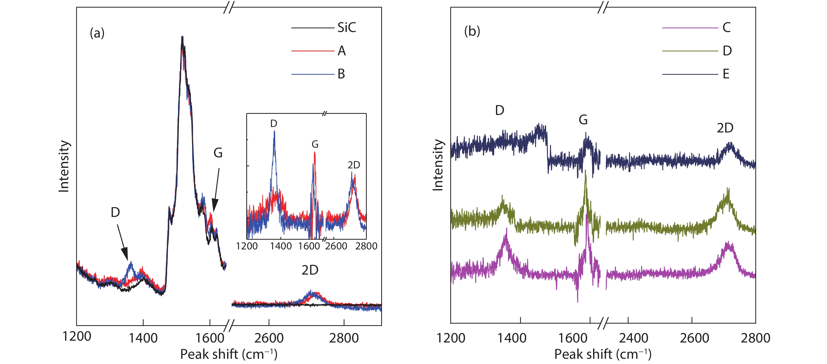
The Raman spectra of the graphene samples A–E and the SiC substrate are shown in Fig. 1. Graphene contains two dominated Raman bands of G-band at ~1582 cm–1 and 2D band at ~2679 cm–1 (the second order of D-band)[
![]()
Figure 1.(Color online) Raman spectra of (a) graphene samples A and B and the SiC substrate, and (b) graphene samples C, D, and E.
The performance of the five graphene gas sensors was measured and their corresponding sensitivity was calculated by[
where R0 is the resistance prior of the device to exposure to the target gas and R is the resistance after exposure to the target gas molecules. Sensor responses for NO2 and NH3 gases, p- and n-type dopants to graphene, are represented in Fig. 2.
![]()
Figure 2.(Color online) Sensor responses for (a, b) NO2 and (c, d) NH3.
As shown in Fig. 2(a), all the graphene sensors show an obvious response to NO2 gas. The sensitivity of the graphene samples shows nearly liner dependence with the NO2 gas concentration at the lower concentration region (400 ppb to 1 ppm), as shown in Fig. 2(b) and Table 2. The response of EG (samples A and B) to NO2 gas is much higher than the QFSEG (samples C and D) and CVD-EG (sample E). Compared with sample A, the defect-engineered sample B shows great improvement in the sensitivity to NO2 gas. The detection limit was calculated by the sensor’s signal processing performance by the following equation[
where rms is the noise (signal to noise ratio at base line). The DL to NO2 gas for samples A and B reached 1 and 2 ppb, respectively, indicating the high sensitivity of the EG samples to NO2 gas. The DL to NO2 gas for samples C, D and E were 60, 70, and 50 ppb, respectively.
QFSEG and CVD-EG samples (samples C, D, and E) show comparable response and DL to NO2 gas. The EG samples (samples A and B) show much higher sensitivity to NO2 gas than the QFSEG and CVD-EG samples. This may be due to the different doping types of the samples: samples A and B are n type doping; samples C, D, and E are p type doping; and, NO2 gas is a well-known p-type dopant to graphene sample.
As illustrated in Fig. 3, a simple model was used to explain the different responses of graphene samples with different doping types (samples A, C/D, and E). The Fermi energies of EG and QFSEG and CVD-EG are different (Fig. 3(a)). The EG samples are n type (Ns = 1 × 1013 cm–2) due to the Fermi level pinning effect of the buffer layer[
![]()
Figure 3.(Color online) Schematic illustration of (a) the Fermi level shift and (b) resistance due to NO2 doping for n-type EG and p-type QFSEG and CVD-EG.
Compared with sample A, the defect-engineered sample B shows a great improvement in the sensitivity to NO2 gas. The response of the graphene sensors to NH3 is not the same with NO2. Only samples A and C show responses to NH3, as shown in Fig. 2(c). Other samples show no obvious response to NH3. These results are consistent with the reported results and first-principles calculations[
4. Conclusions
Epitaxial graphene, quasi-free-standing graphene, and CVD epitaxial graphene samples on SiC substrates are used to fabricate gas sensors. The epitaxial graphene shows the highest sensitivity to NO2 gas. This can be explained by the doping type and resistance-carrier density relation. The defect-engineered sample shows improved sensitivity to NO2 with response of 105.1% to 4 ppm NO2, which is consistent with the DFT calculations that both of the adsorption energies and charge transfer increased. The samples show weak response to NH3 due to the small charge transfer. Our results show the application potential of epitaxial graphene on SiC to NO2 gas detection.
Acknowledgements
This work was supported by the National Natural Science Foundation of China (61674131 and 61306006).
References
[1] F Schedin, A K Geim, S V Morozov et al. Detection of individual gas molecules adsorbed on graphene. Nat Mater, 6, 652(2007).
[2] A K Geim, K S Novoselov. The rise of graphene. Nat Mater, 6, 183(2007).
[3] K S Novoselov, V I Falko, L Colombo et al. A roadmap for graphene. Nature, 490, 192(2012).
[4] S S Varghese, S Lonkar, K K Singh et al. Recent advances in graphene based gas sensors. Sens Actuators B, 218, 160(2015).
[5] Y Dan, Y Lu, N J Kybert et al. Intrinsic response of graphene vapor sensors. Nano Lett, 9, 1472(2009).
[6] S Rumyantsev, G Liu, M S Shur et al. Selective gas sensing with a single pristine graphene transistor. Nano Lett, 12, 2294(2012).
[7] G Lee, G Yang, A Cho et al. Defect-engineered graphene chemical sensors with ultrahigh sensitivity. Phys Chem Chem Phys, 18, 14198(2016).
[8] A K Singh, M A Uddin, J T Tolson et al. Electrically tunable molecular doping of graphene. Appl Phys Lett, 102, 043101(2013).
[9] K Toda, R Furue, S Hayami. Recent progress in applications of graphene oxide for gas sensing: A review. Anal Chim Acta, 878, 43(2015).
[10] W Li, X Geng, Y Guo et al. Reduced graphene oxide electrically contacted graphene sensor for highly sensitive nitric oxide detection. ACS Nano, 5, 6955(2011).
[11] M W K Nomani, R Shishir, M Qazi et al. Highly sensitive and selective detection of NO2 using epitaxial graphene on 6H-SiC. Sens Actuators B, 150, 301(2010).
[12] R Pearce, T Iakimov, M Andersson et al. Epitaxially grown graphene based gas sensors for ultra sensitive NO2 detection. Sens Actuators B, 155, 451(2011).
[13] I Iezhokin, P Offermans, S H Brongersma et al. High sensitive quasi freestanding epitaxial graphene gas sensor on 6H-SiC. Appl Phys Lett, 103, 053514(2013).
[14] A A Lebedev, S P Lebedev, S N Novikov et al. Supersensitive graphene-based gas sensor. Tech Phys, 61, 3, 453(2016).
[15] S Novikov, N Lebedeva, A Satrapinski. Graphene based sensor for environmental monitoring of NO2. J Sen, 2015, 7(2015).
[16] K Wetchakun, T Samerjai, N Tamaekong et al. Semiconducting metal oxides as sensors for environmentally hazardous gases. Sens Actuators B, 160, 580(2011).
[17] T Zhang, S Mubeen, N V Myung et al. Recent progress in carbon nanotube-based gas sensors. Nanotechnology, 19, 332001(2008).
[18] B Kumar, K Min, M Bashirzadeh et al. The role of external defects in chemical sensing of graphene field-effect transistors. Nano Lett, 13, 1962(2013).
[19] M G Chung, D H Kim, H M Lee et al. Graphene-based composite materials for chemical sensor application. Sens Actuators B, 166/16, 172(2012).
[20] C Yu, J Li, Q B Liu et al. Buffer layer induced band gap and surface low energy optical phonon scattering in epitaxial graphene on SiC (0001). Appl Phys Lett, 102, 013107(2013).
[21] C Yu, Q B Liu, J Li et al. Preparation and electrical transport properties of quasi free standing bilayer graphene on SiC (0001) substrate by H intercalation. Appl Phys Lett, 105, 183105(2014).
[22] O Pankratov, S Hensel, M Bockstedte. Electron spectrum of epitaxial graphene monolayers. Phys Rev B, 82, 121416(2010).
[23] J Ristein, S Mammadov, T Seyller. Origin of doping in quasi-free-standing graphene on silicon carbide. Phys Rev Lett, 108, 246104(2012).
[24] T Ciuk, W Strupinski. Charge carrier concentration and offset voltage in quasi-free-standingmonolayer chemical vapor deposition graphene on SiC. Carbon, 93, 1042(2015).
[25] T Ciuk, P Caban, W Strupinski. Statistics of epitaxial graphene for Hall effect sensors. Carbon, 101, 431e438(2016).
[26] A C Ferrari. Raman spectroscopy of graphene and graphite: Disorder, electron–phonon coupling, doping and nonadiabatic effects. Solid State Commun, 143, 47(2007).
[27] Y R Choi, Y G Yoon, K S Choi et al. Role of oxygen functional groups in graphene oxide for reversible room-temperature NO2 sensing. Carbon, 91, 178(2015).
[28] M Portail, A Michon, S Vezian et al. Growth mode and electric properties of graphene and graphitic phase grown by argon-propane assisted CVD on 3C-SiC/Si and 6H-SiC. J Cryst Growth, 349, 27(2012).
[29] D Waldmann, J Jobst, F Speck et al. Bottom-gated epitaxial graphene. Nat Mater, 10, 357(2011).
[30] Y H Zhang, Y B Chen, K G Zhou et al. Improving gas sensing properties of graphene by introducing dopants and defects: a first-principles study. Nanotechnology, 20, 185504(2009).

Set citation alerts for the article
Please enter your email address
© Copyright 2018-2021 | Chinese Laser Press. All Rights Reserved 沪ICP备15018463号-20