
Yong Li, Huifang Zhang, Qiong Wu, Ying He, Yan Wang. Theoretical Analysis of Single Dielectric Loaded Two-Sheet Graphene Symmetric Surface Plasmon Waveguide[J]. Laser & Optoelectronics Progress, 2019, 56(20): 202413
- Laser & Optoelectronics Progress
- Vol. 56, Issue 20, 202413 (2019)
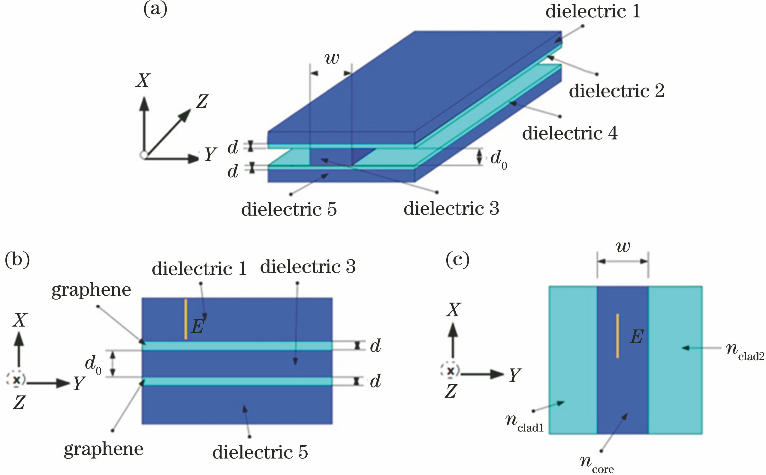
Fig. 1. DLTGSSPW. (a) Theoretical model; (b) equivalent five-layer planar waveguide structure of D1/G/D3/G/D5; (c) equivalent three-layer planar waveguide structure
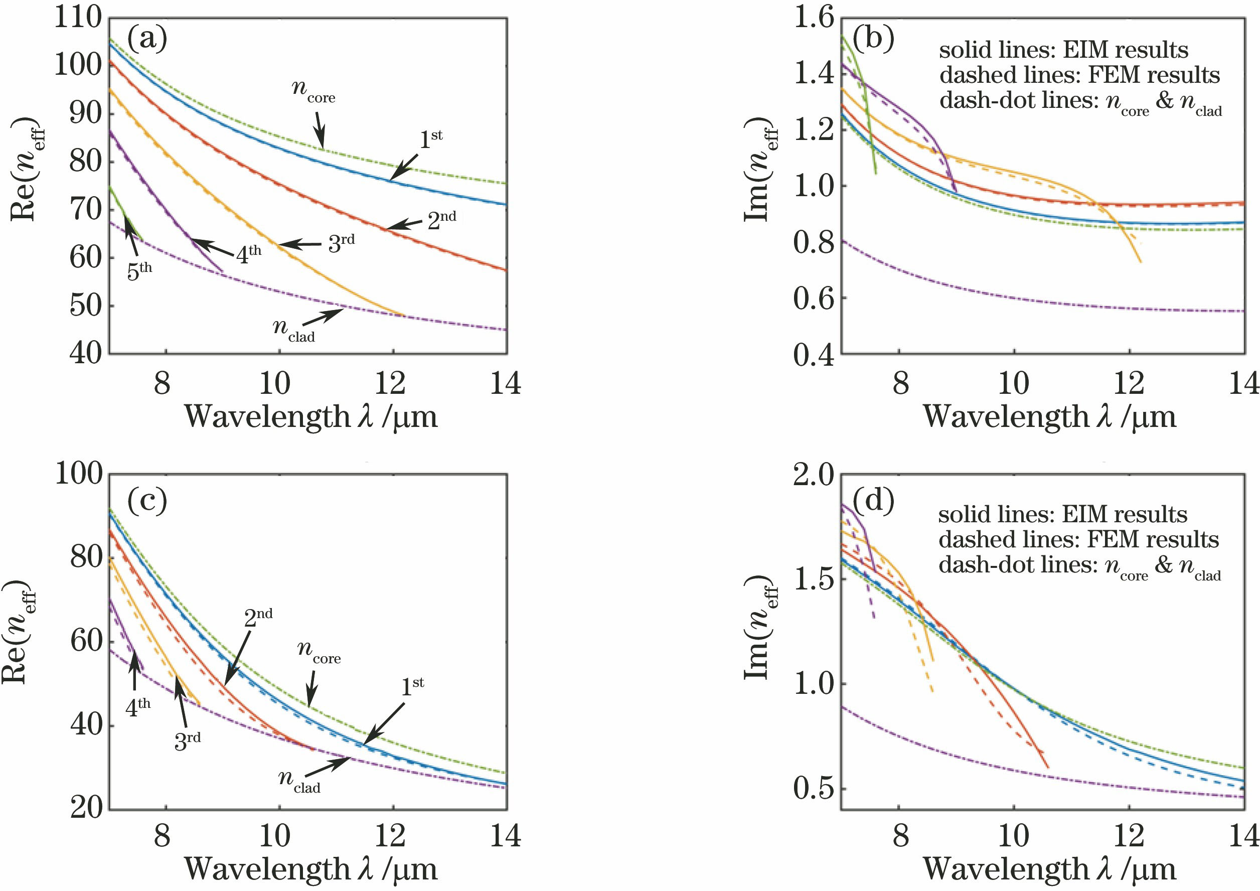
Fig. 2. Effective refractive index of GSPP mode versus wavelength in DLTGSSPW with w=200 nm and d0=30 nm. (a) Symmetric mode, Re(neff); (b) symmetric mode, Im(neff); (c) anti-symmetric mode, Re(neff); (d) anti-symmetric mode, Im(neff)
Fig. 3. Mode patterns under w=200 nm and d0=30 nm. 3rd order symmetric GSPP mode at (a) λ=8 μm and (b) λ=10 μm; 1st order (c) symmetric and (d) anti-symmetric GSPP modes at λ=9.6 μm
Fig. 4. Effective refractive index of GSPP mode versus dielectric bar width in DLTGSSPW with λ=8 μm and d0=30 nm. (a) Symmetric mode, Re(neff); (b) symmetric mode, Im(neff); (c) anti-symmetric mode, Re(neff); (d) anti-symmetric mode, Im(neff)
Fig. 5. Mode patterns of 2nd order symmetric GSPP mode in DLTGSSPW with λ=8 μm and d0=30 nm.(a) w=80 nm; (b) w=150 nm
Fig. 6. Effective refractive index of GSPP mode versus dielectric bar height in DLTGSSPW with λ=8 μm and w=200 nm. (a) Symmetric mode, Re(neff); (b) symmetric mode, Im(neff); (c) anti-symmetric mode, Re(neff); (d) anti-symmetric mode, Im(neff)
Fig. 7. Mode patterns in DLTGSSPW with w=200 nm and λ=8 μm. (a) 1st order symmetric GSPP mode, d0=10 nm; (b) 1st order anti-symmetric GSPP mode, d0=10 nm; (c) 1st order symmetric GSPP mode, d0=100 nm; (d) 1st order anti-symmetric GSPP mode, d0=100 nm; (e) 4th order symmetric GSPP mode, d0=20 nm; (f) 4th order symmetric GSPP mode, d0=80 nm

Set citation alerts for the article
Please enter your email address
© Copyright 2018-2021 | Chinese Laser Press. All Rights Reserved 沪ICP备15018463号-20