
Shu Zong, Dongwen Zeng, Wen Yuan, Guiqiang Liu, Zhengqi Liu, "Recent advances on perfect light absorbers and their promise for high-performance opto-electronic devices [Invited]," Chin. Opt. Lett. 20, 073603 (2022)
- Chinese Optics Letters
- Vol. 20, Issue 7, 073603 (2022)
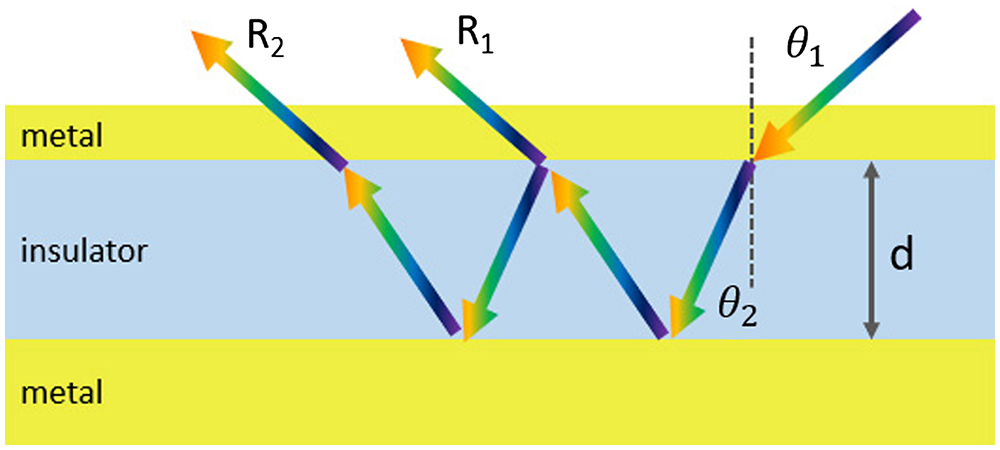
Fig. 1. Schematic of the resonant FP cavity.
![(a) Schematic of the MoS2-based PA. (b) Simulated results of the monolayer MoS2-based PAs[34]. (c) Illustration of the WS2 MPAs and the unit cell. (d) Absorption and reflection spectra of the MPAs[35].](/richHtml/col/2022/20/7/073603/img_002.jpg)
Fig. 2. (a) Schematic of the MoS2-based PA. (b) Simulated results of the monolayer MoS2-based PAs[34]. (c) Illustration of the WS2 MPAs and the unit cell. (d) Absorption and reflection spectra of the MPAs[35].
Fig. 3. (a) Schematic of the graphene MPA and the unit cell. (b) Absorption, transmission, and reflection spectra of the graphene MPA[53].
Fig. 4. (a) Schematic of the MLPA. (b) Reflection and absorption spectra of the structure. (c) Normalized electric field intensity distributions of the absorption peaks at λ1–λ4, respectively[54]. (d) Illustration of the MPAs. (e) The equivalent circuit model of the absorber[55].
Fig. 5. (a) Schematic of broadband titanium nitride disordered MAs[100]. (b) Schematic of a nanostructured wideband light absorber prepared on top of a commercial thermoelectric device. (c) The extinction spectra of the flat film and two nanostructures with radius of r = 198 nm and 201 nm are measured in the visible and short-wave infrared regions. (d) Extinction spectra of the flat film, nanostructure, and nanostructure with surface roughness are simulated[105].
Fig. 6. (a) Schematic of the absorber and the corresponding cross-section view. (b) The absorption spectra of the MA with optimized geometry[106]. (c) Schematic diagram of Al-ZnS multilayer sawtooth absorber and a single structural unit. (d) The absorption spectra of TM and TE polarized light incidence and hyperbolic metamaterials with TM polarized light incidence under effective medium theory are studied[77].
Fig. 7. (a) Illustration of an independent tunable multipurpose absorber using a monolayer metal-graphene metamaterial. (b) Top view of a single structural unit. (c) Absorption spectra obtained by Ef1 independently. (d) Absorption spectra obtained by Ef2 independently[128]. (e) Schematic diagram of polarized light incident into the absorber structural unit. (f) Absorption of T < Tc and T > Tc is simulated, respectively[137]. (g) The proposed 3D schematic diagram of DTA based on VO2. (h) Absorption contrast of each characteristic wavelength is calculated when the structural parameters are w = 0–200 nm, h1 = 0–100 nm, h2 = 5–100 nm, h3 = 200 nm, and p = 200 nm. The device structure parameters corresponding to each characteristic wavelength are shown in the inset[141].
Fig. 8. (a) Schematic and section in 3D of the solar absorber designed. (b) Absorption spectra of the solar absorber, MSM structure, and MSM structure without the ITO layer. (c) Standard spectrum and absorption spectrum of the solar absorber at AM 1.5. (d) Solar energy absorption and leakage in the full spectrum of solar energy[67].
Fig. 9. (a) Basic unit and structural parameters of the absorber. (b) Absorption of the nanocones composed of Bi2Te3, Cr, Si, and Si covered with Cr layer, respectively[172].
Fig. 10. (a) Schematic 3D view of the proposed graphene structure. (b) The front view of a unit cell of the structure. (c) Reflection spectra of the graphene structure in different environment media. (d) The corresponding S[190].
Fig. 11. (a) Absorption spectra for different graphene chemical potentials and temperatures. Schematic of ON and OFF states[197]. (b) Illustration of the switchable state[141]. (c) The reflection spectra of the designed metasurface at 60°C (insulator phase) and 88°C (metallic phase)[201].
Fig. 12. (a) Illustration of asymmetric FP nanocavity absorber. Reproduced with permission from Ref. [216] Copyright 2021, American Chemical Society. (b) Measured (solid line) and simulated (dashed line) reflectance spectra and corresponding colors at different FP cavity thicknesses[216]. (c) Illustration of the proposed VO2 dynamic structural colors. The reflected light varies with Ag film and VO2 thickness at (d) 30°C and (e) 100°C[217].
|
Table 1. Comparison of Representative Theoretical and Experimental Works on the Topic of Ultra-Broadband MPAs in Recent Years
|
Table 2. The Advantages and Disadvantages of Opto-Electronic Devices Based on MPA


Set citation alerts for the article
Please enter your email address

© Copyright 2018-2021 | Chinese Laser Press. All Rights Reserved 沪ICP备15018463号-20