
Shu Zong, Dongwen Zeng, Wen Yuan, Guiqiang Liu, Zhengqi Liu, "Recent advances on perfect light absorbers and their promise for high-performance opto-electronic devices [Invited]," Chin. Opt. Lett. 20, 073603 (2022)
- Chinese Optics Letters
- Vol. 20, Issue 7, 073603 (2022)
Abstract
1. Introduction
An electromagnetic wave absorber is a device that can absorb and annihilate electromagnetic waves, which is widely used in various fields of military, science and technology, and people’s livelihood. Therefore, the development of perfect absorption and functional devices is always a hot spot in the physics community. Metamaterials are artificially designed structures that exhibit supernormal physical properties not found in natural materials. The resonance excited by its unique geometric structure of united cell enables it to have a strong interaction with electromagnetic fields. The ability makes it widely used in the fields of antenna enhancement[
In this review, the first part summarizes the latest progress in PAs and introduces five directions of narrow-band, dual-band, multi-band, broadband, and tunable absorption based on the differences in the applications of different absorbers. We summarize the shortcomings of the previous PAs and the latest improvements. In the second part, we introduce the application of perfect absorption in solar cells, sensors, switches, and structural colors. Finally, the main challenges and prospects are discussed.
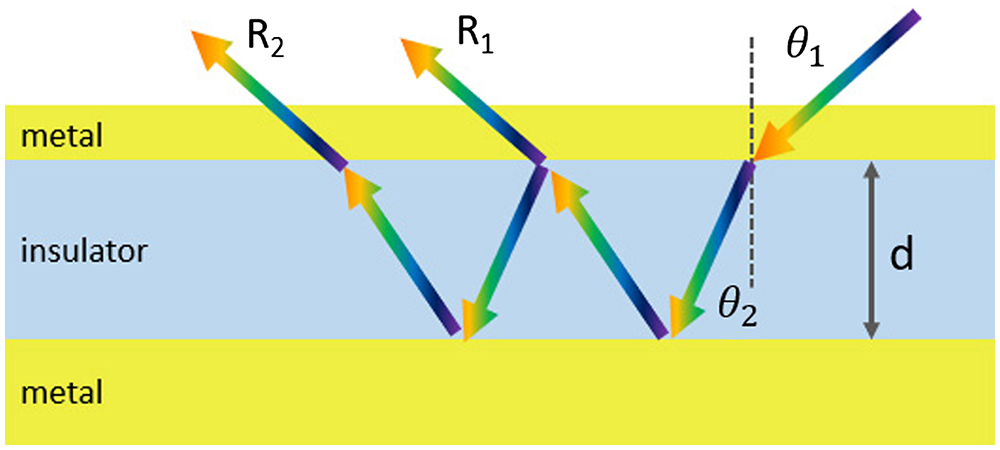
2. The Latest Development of Perfect Absorbers
The traditional absorbers based on Fabry–Perot (FP) resonance (Fig. 1) have played an indispensable role in the development of MPA, which generally consists of an MIM structure with multiple layers. The MIM structure is composed of a metal mirror on the top, an insulator in the middle, and a metal bottom plate; for example, the first MPA is composed of a metal ring resonator, a dielectric layer, and a metal wire. For the first MPA, the electrical response is excited by the strong coupling between the metal ring resonator and the incident electric field, and magnetic coupling is achieved by anti-parallel currents between the metal wire and the metal ring resonator center line[
Sign up for Chinese Optics Letters TOC. Get the latest issue of Chinese Optics Letters delivered right to you!Sign up now
![]()
Figure 1.Schematic of the resonant FP cavity.
2.1. The latest development of narrow-band perfect absorbers
The first, to the best of our knowledge, perfect metamaterial absorber (MA) proposed by Landy et al. is a relative narrow-band absorber[
![]()
Figure 2.(a) Schematic of the MoS2-based PA. (b) Simulated results of the monolayer MoS2-based PAs[
Compared to the single-band absorber, multi-band light absorption is more desired for high-integration opto-electronic applications due to its multiple resonant absorption bands. In the next section, we will introduce the latest development of dual-band and multi-band PAs.
2.2. The latest development of dual-band and multi-band perfect absorbers
Perfect absorption of dual-band and multi-band spectra is desirable for many applications. Compared with a single absorption peak, multi-band optical absorption is more suitable for highly integrated opto-electronic applications, such as multi-spectral detection[
![]()
Figure 3.(a) Schematic of the graphene MPA and the unit cell. (b) Absorption, transmission, and reflection spectra of the graphene MPA[
As early as 2016, Liu et al.[
![]()
Figure 4.(a) Schematic of the MLPA. (b) Reflection and absorption spectra of the structure. (c) Normalized electric field intensity distributions of the absorption peaks at λ1–λ4, respectively[
2.3. The latest development of ultra-wideband perfect absorbers
The technologies of broadband spectral absorption from visible light to infrared light have gained a lot of attention, due to its applications related to energy[
A disordered gold nanoparticles multilayer structure absorber was proposed, which was deposited on a
![]()
Figure 5.(a) Schematic of broadband titanium nitride disordered MAs[
It is innovative for the wideband absorber to integrate into commercial thermoelectric devices. Nevertheless, a critical problem is that although the bandwidth of the absorber meets the requirements, the average absorption rate over the whole broadband range is not high.
In recent years, metal grating MAs have attracted much attention because of their simple and cost-effective design. Cai et al.[
![]()
Figure 6.(a) Schematic of the absorber and the corresponding cross-section view. (b) The absorption spectra of the MA with optimized geometry[
In addition, we sorted out a table of absorption efficiency of light absorbers of various materials by comprehensively reviewing literatures on broadband light absorption in the past two years, as shown in Table 1.
| Work by | Device Configuration | Bandwidth | Absorptance | Reference |
|---|---|---|---|---|
| Chen et al. (2021) | 900–1900 nm | [ | ||
| Cai et al. (2020) | 300–2100 nm | 98.3% | [ | |
| Yue et al. (2020) | Al and ZnS | 0.2–15 µm (UV-LWIR) | Angle of | [ |
| Liu et al. (2020) | Si, Ti, | 405–1505 nm (vis-to-NIR) | 95.14% | [ |
| Zhang et al. (2020) | 0.5–1.8 µm (vis-to-NIR) | 95.6% | [ | |
| Ijaz et al. (2021) | ZrN | 400–800 nm 280–2200 nm | [ | |
| Zhao et al. (2020) | Ge and | 450–750 nm (vis) | 97.4% | [ |
| Dong et al. (2021) | ITO and | 300–1000 nm | Average 96%, | [ |
| Zhong et al. (2021) | Ti | 0.38–2.0 µm (vis-to-NIR) | Average 93.6%, maximum 98.9% | [ |
| Guo et al. (2021) | TiN | 100–2500 nm (vis-to-NIR) | Average 96.11% | [ |
| Zhou et al. (2021) | Ti and Si (MIM) | 400–2500 nm (vis-to-NIR) | Average 93.8%, maximum 99.8% | [ |
| Qian et al. (2021) | 400–1800 nm | 96.1% | [ | |
| Piao et al. (2021) | TiN | 300–2500 nm | [ | |
| Zhang et al. (2020) | W and | 300–1200 nm | TE: average 96%, maximum 99.4%; TM: average 91%, maximum 99.8% | [ |
Table 1. Comparison of Representative Theoretical and Experimental Works on the Topic of Ultra-Broadband MPAs in Recent Years
2.4. Recent advances in tunable perfect absorbers
Achieving controllable and compact perfect absorption has great prospects in nanophotonic systems. However, most of the absorbers reported in recent years were focused on metal or lossy media, leading to the lack of structural and behavior flexibility. The absorption properties are fixed and cannot be adjusted in a controllable way[
![]()
Figure 7.(a) Illustration of an independent tunable multipurpose absorber using a monolayer metal-graphene metamaterial. (b) Top view of a single structural unit. (c) Absorption spectra obtained by Ef1 independently. (d) Absorption spectra obtained by Ef2 independently[
Although these absorbers based on van der Waals (VDW) materials can be tuned, their operating bandwidth is limited. It is troublesome to utilize the absorber because graphene always requires an external electrical bias[
3. Application of the Perfect Absorber
In the past decade, MPA showed notable and excellent property and emerged with extensive applications[
| Opto-Electronic Devices | Advantage | Disadvantage | Reference |
|---|---|---|---|
| Solar cell | High efficiency | Expensiveness | [ |
| Sensor | Sensitivity | Complex structure | [ |
| Switch | Integration; high switching ratio | High preparation requirements | [ |
| Structural color | Stability; environmental protection | High cost; low production efficiency | [ |
Table 2. The Advantages and Disadvantages of Opto-Electronic Devices Based on MPA
3.1. Solar energy harvesting
Solar energy, as a kind of clean and renewable energy, has been a popular research object because of its wide application. Solar cells[
In recent years, the classic MIM structure of the absorber for its perfect absorption also is often used in solar cells. However, this film stack PA mainly absorbs light into two layers of metal heat (ohmic losses), lacking the ability to make solar energy directly from the light into an electric current[
Therefore, light capture has become one of the main topics of thin film solar cells. GaAs has become a good competitor in recent years due to its unique optical properties and high conversion efficiency[
![]()
Figure 8.(a) Schematic and section in 3D of the solar absorber designed. (b) Absorption spectra of the solar absorber, MSM structure, and MSM structure without the ITO layer. (c) Standard spectrum and absorption spectrum of the solar absorber at AM 1.5. (d) Solar energy absorption and leakage in the full spectrum of solar energy[
Freshwater is indispensable to human daily life, but the freshwater resources on earth are very limited. Solving the clean water crisis is an important challenge for human sustainable development. During the study of MPA, the researchers found that the light energy absorbed by the MPA was converted into heat energy due to the ohmic loss of the metal and dielectric loss. Based on this photothermal conversion phenomenon, in the field of perfect solar energy absorption, many efforts have been made to realize high-performance absorbers that can drive seawater evaporation and desalination. Among many metamaterials to achieve perfect broadband absorption, nanocone structured absorbers have attracted attention because of their ease of manufacture and simple principle of achieving broadband absorption.
Wang et al.[
![]()
Figure 9.(a) Basic unit and structural parameters of the absorber. (b) Absorption of the nanocones composed of Bi2Te3, Cr, Si, and Si covered with Cr layer, respectively[
3.2. Sensors
Sensor is a device that can feel the specified measurement and convert it into usable signals according to certain rules. It is used to obtain information that cannot be directly obtained by human senses. It is widely used in industrial production[
Graphene has attracted more and more attention in recent years due to its excellent electrical, mechanical, and chemical properties. In optical sensors, absorbers with ultra-narrow bandwidth have broad application prospects. Yan et al. proposed an ultra-narrow-band PA by coating graphene-dielectric-metal with a dielectric grating. The structure of the absorber is shown in Figs. 10(a) and 10(b). The ultra-narrow band is generated by the light dissipation of graphene and the GMR of the dielectric grating. When the RI increases from 1.00 to 1.04, the relationship between the resonant wavelength and RI is shown in Figs. 10(c) and 10(d). High performance of sensing with
![]()
Figure 10.(a) Schematic 3D view of the proposed graphene structure. (b) The front view of a unit cell of the structure. (c) Reflection spectra of the graphene structure in different environment media. (d) The corresponding S[
3.3. Switches
Optical switching is a kind of process in which a certain parameter of light (intensity, wavelength, polarization, etc.) is changed from one state to another state rapidly, reversibly, and discontinuously under a certain drive[
![]()
Figure 11.(a) Absorption spectra for different graphene chemical potentials and temperatures. Schematic of ON and OFF states[
In addition, the manufacturing process of the DTA is compatible with CMOS technology. DTA-based optical switches are also an important development direction. In recent years,
3.4. Structural colors
Colors play a most indispensable role in our visual world. In daily life, the colors we often use mainly come from various pigments. Unlike everyday pigments, the large backs of many beetles and the wings of butterflies can also show various colors in nature. The main causes of this phenomenon are interference and diffraction of light. We call these structural colors that can be produced by artificially controlling structural morphology and geometry. The generation of structural colors by MPA is realized because the researchers reasonably designed the MPA, and the wavelength of the reflected wave is manually controlled in the visible band.
MPA-based structural colors have a wide range of applications in anti-counterfeiting[
![]()
Figure 12.(a) Illustration of asymmetric FP nanocavity absorber. Reproduced with permission from Ref. [216] Copyright 2021, American Chemical Society. (b) Measured (solid line) and simulated (dashed line) reflectance spectra and corresponding colors at different FP cavity thicknesses[
4. Conclusions and Future Outlook
In this review, we summarized some of the research developments and applications of PAs in the past few years. In the past two years, the emergence of new concepts and new methods has led to the rapid development of PAs and has shown great potential in application. Great attention has been attracted since MPAs were proposed in 2008. The latest developments of PAs with single-band, dual-band, multi-band, wide-band, narrow-band, and tunable light absorption have been summarized to show their unique characteristics and applications. The shortcomings of the related PAs and the latest improvements were introduced as well. Moreover, we further introduced the application of perfect absorption in solar cells, sensor switches, and structural colors. We also presented the main challenges and prospects in these fields. We believe that novel PAs for wide applications in opto-electronic fields will continuously progress with breakthrough advances in future technology and science.
However, in actual industrial production, we must consider the significant factors for all absorbers. First of all, in most absorbers, noble metals, such as gold and Ag, are often used as substrates or resonators. For some large-scale optical devices, due to the high ohmic loss and heat generation, the aim of cost-control, and the intrinsic characteristic of scarce resources, using noble metals as the substrate will extremely hamper the wide applications. That is, the new resonant materials should be considered for the plasmonic or plasmon-like materials, such as the high-index dielectrics and doped semiconductors. Secondly, complex patterned antenna layers are widely designed and used in the absorbers, even with a need of size down to the nanometer scale. Therefore, multi-step and high-cost lithography methods such as FIB, electron beam lithography (EBL), and reactive ion etching (RIE) are used as typical methods. The high cost and low yield of these technologies will limit the application of PAs. In addition, the solar absorber needs to be insensitive to polarization and incident angle and also requires high stability for the temperature and chemical surroundings. In the development of optical switches, not only temperature-controlled optical switches and electronically controlled optical switches, but also light-controlled all-optical switches, all have the need for the realization of the concept of higher-speed switch response and high signal-to-noise ratio. To sum up, a lot of great efforts have been made for the development of the PAs in these years, leading to the emergence of a series of new science and technologies for applications in opto-electronic devices. With the rapid development, we have reason to believe that the PA has a bright future.
References
[1] J. X. Li, S. W. Yang, C. H. Wang, W. T. Joines, Q. H. Liu. Metamaterial cavity for the isolation enhancement of closely positioned dual-polarized relay antenna arrays. Microw. Opt. Techn. Lett., 59, 857(2017).
[2] S. K. Patel, K. H. Shah, Y. P. Kosta. Multilayer liquid metamaterial radome design for performance enhancement of microstrip patch antenna. Microw. Opt. Techn. Lett., 60, 600(2018).
[3] C. M. Saleh, D. Bensafieddine, E. M. Laamari, M. Bouzouad. A zero-index metamaterial single layer superstrate for patch antenna gain enhancement. Acta Phys. Pol., 128, B307(2015).
[4] C. P. Scarborough, Z. H. Jiang, D. H. Werner, C. Rivero-Baleine, C. Drake. Experimental demonstration of an isotropic metamaterial super lens with negative unity permeability at 8.5 MHz. Appl. Phys. Lett., 101, 014101(2012).
[5] Y. H. Zhao, A. A. Nawaz, S. C. S. Lin, Q. Z. Hao, B. Kiraly, T. J. Huang. Nanoscale super-resolution imaging via a metal–dielectric metamaterial lens system. J. Phys. D, 44, 415101(2011).
[6] X. J. Huang, H. L. Yang, Z. Y. Shen, J. Chen, H. I. Lin, Z. T. Yu. Water-injected all-dielectric ultra-wideband and prominent oblique incidence metamaterial absorber in microwave regime. J. Phys. D, 50, 385304(2017).
[7] C. L. Xu, B. K. Wang, M. B. Yan, Y. Q. Pang, W. J. Wang, Y. Y. Meng, J. F. Wang, S. B. Qu. An optical-transparent metamaterial for high-efficiency microwave absorption and low infrared emission. J. Phys. D, 53, 135109(2019).
[8] N. Landy, S. Sajuyigbe, J. Mock, D. Smith, W. Padilla. Perfect metamaterial absorber. Phys. Rev. Lett., 100, 207402(2008).
[9] J. Bucinskas, L. Nickelson, V. Shugurovas. Microwave scattering and absorption by a multilayered lossy metamaterial-glass cylinder. Prog. Electromagn. Res., 105, 103(2010).
[10] W. Luo, X. Wang, S. Wang, X. Wang, Z. Liu, L. Li, F. Hu, Y. Wen, J. Zhou. Miniaturization of dielectric ceramic-based metamaterial perfect absorber. Appl. Phys. Lett., 120, 013502(2022).
[11] J. Y. Jung, J. Lee, D. G. Choi, J. H. Choi, J. H. Jeong, E. S. Lee, D. P. Neikirk. Wavelength-selective infrared metasurface absorber for multispectral thermal detection. IEEE Photonics J., 7, 6804210(2015).
[12] S. W. Dai, D. Zhao, Q. Li, M. Qiu. Double-sided polarization-independent plasmonic absorber at near-infrared region. Opt. Express, 21, 13125(2013).
[13] D. Wu, R. F. Li, Y. M. Liu, Z. Y. Yu, L. Yu, L. Chen, C. Liu, R. Ma, H. Ye. Ultra-narrow band perfect absorber and its application as plasmonic sensor in the visible region. Nanoscale Res. Lett., 12, 427(2017).
[14] M. L. Li, B. Muneer, Z. X. Yi, Q. Zhu. A broadband compatible multispectral metamaterial absorber for visible, near-infrared, and microwave bands. Adv. Opt. Mater., 6, 1701238(2018).
[15] B. Grzeskiewicz, A. Sierakowski, J. Marczewski, N. Palka, E. Wolarz. Polarization-insensitive metamaterial absorber of selective response in terahertz frequency range. J. Opt., 16, 105104(2014).
[16] H. Kong, G. F. Li, Z. M. Jin, G. H. Ma, Z. W. Zhang, C. L. Zhang. Polarization-independent metamaterial absorber for terahertz frequency. J. Infrared Millim. Terahertz Waves, 33, 649(2012).
[17] X. Liu, T. Tyler, T. Starr, A. F. Starr, N. M. Jokerst, W. J. Padilla. Taming the blackbody with infrared metamaterials as selective thermal emitters. Phys. Rev. Lett., 107, 045901(2011).
[18] M. L. Hakim, T. Alam, A. F. Almutairi, M. F. Mansor, M. T. Islam. Polarization insensitivity characterization of dual-band perfect metamaterial absorber for K band sensing applications. Sci. Rep., 11, 17829(2021).
[19] J. Luo, H. Chu, R. Peng, M. Wang, J. Li, Y. Lai. Ultra-broadband reflectionless Brewster absorber protected by reciprocity. Light Sci. Appl., 10, 89(2021).
[20] F. Wu, X. H. Wu, S. Y. Xiao, G. H. Liu, H. J. Li. Broadband wide-angle multilayer absorber based on a broadband omnidirectional optical Tamm state. Opt. Express, 29, 23976(2021).
[21] J. Luo, H. Chu, R. Peng, M. Wang, J. Li, Y. Lai. Ultra-broadband reflectionless Brewster absorber protected by reciprocity. Light Sci. Appl., 10, 89(2021).
[22] Y. Zhou, Z. Qin, Z. Liang, D. Meng, H. Xu, D. R. Smith, Y. Liu. Ultra-broadband metamaterial absorbers from long to very long infrared regime. Light Sci. Appl., 10, 138(2021).
[23] C. M. Watts, X. Liu, W. J. Padilla. Metamaterial electromagnetic wave absorbers. Adv. Mater., 24, 98(2012).
[24] D. Yevick, D. J. Thomson. Impedance-matched absorbers for finite-difference parabolic equation algorithms. J. Acoust. Soc. Am., 107, 1226(2000).
[25] N. Luhmann, D. Hoj, M. Piller, H. Kähler, M.-H. Chien, R. G. West, U. L. Andersen, S. Schmid. Ultrathin 2 nm gold as impedance-matched absorber for infrared light. Nat. Commun., 11, 2161(2020).
[26] M. Y. Pan, L. B. Wang, S. L. Dou, J. P. Zhao, H. B. Xu, B. Wang, L. P. Zhang, X. B. Li, L. Pan, Y. Li. Recent advances in colloidal photonic crystal-based anti-counterfeiting materials. Crystals, 9, 417(2019).
[27] C. Jung, Y. Yang, J. Jang, T. Badloe, T. Lee, J. Mun, S. W. Moon, J. J. Rho. Near-zero reflection of all-dielectric structural coloration enabling polarization-sensitive optical encryption with enhanced switchability. Nanophotonics, 10, 919(2021).
[28] G. H. Rui, C. C. Ding, B. Gu, Q. Q. Gan, Q. W. Zhan, Y. P. Cui. Symmetric Ge2Sb2Te5 based metamaterial absorber induced dynamic wide-gamut structural color. J. Opt., 22, 085003(2020).
[29] S. U. Kim, S. H. Lee, I. H. Lee. Generation of intensity-tunable structural color from helical photonic crystals for full color reflective-type display. Sci. Adv., 4, 8829(2018).
[30] S. L. Li, M. C. Panmai, S. L. Tie, Y. Xu, J. Xiang, S. Lan. Regulating disordered plasmonic nanoparticles into polarization sensitive metasurfaces. Nanophotonics, 10, 1553(2021).
[31] H. Z. Zhu, Q. Li, C. N. Tao, Y. Hong, Z. Q. Xu, W. D. Shen, S. Kaur, P. Ghosh, M. Qiu. Multispectral camouflage for infrared, visible, lasers and microwave with radiative cooling. Nat. Commun., 12, 1805(2021).
[32] D. J. Ironside, R. Salas, P. Y. Chen, K. Q. Le, A. Alu, S. R. Bank. Enhancing THz generation in photomixers using a metamaterial approach. Opt. Express, 27, 9481(2019).
[33] R. M. Saadabad, L. Huang, A. E. Miroshnichenko. Polarization-independent perfect absorber enabled by quasibound states in the continuum. Phys. Rev. B, 104, 235405(2021).
[34] J. F. Zhang, Q. L. Hong, J. L. Zou, Q. Meng, S. Q. Qin, Z. H. Zhu. Ultra-narrowband visible light absorption in a monolayer MoS2 based resonant nanostructure. Opt. Express, 28, 27608(2020).
[35] Z. B. Li, X. A. Sun, C. R. Ma, J. Li, X. P. Li, B. O. Guan, K. Chen. Ultra-narrow-band metamaterial perfect absorber based on surface lattice resonance in a WS2 nanodisk array. Opt. Express, 29, 27084(2021).
[36] J. Xiang, M. Panmai, S. W. Bai, Y. H. Ren, G. C. Li, S. L. Li, J. Liu, J. T. Li, M. X. Zeng, J. C. She, Y. Xu, S. Lan. Crystalline silicon white light sources driven by optical resonances. Nano Lett., 21, 2397(2021).
[37] Y. T. Chen, J. Dai, M. Yan, M. Qiu. Metal-insulator-metal plasmonic absorbers: influence of lattice. Opt. Express, 22, 30807(2014).
[38] B. Gerislioglu, L. Dong, A. Ahmadivand, H. Hu, P. Nordlander, N. J. Halas. Monolithic metal dimer-on-film structure: new plasmonic properties introduced by the underlying metal. Nano Lett., 20, 2087(2020).
[39] M. Pan, Z. C. Su, Z. F. Yu, P. H. Wu, H. G. Jile, Z. Yi, Z. Q. Chen. A narrowband perfect absorber with high Q-factor and its application in sensing in the visible region. Results Phys., 19, 103415(2020).
[40] D. Hu, T. H. Meng, H. Y. Wang, Y. K. Ma, Q. F. Zhu. Ultra-narrow-band terahertz perfect metamaterial absorber for refractive index sensing application. Results Phys., 19, 103567(2020).
[41] A. Vazquez-Guardado, M. Money, N. Mckinney, D. Chanda. Multi-spectral infrared spectroscopy for robust plastic identification. Appl. Opt., 54, 7396(2015).
[42] X. L. Wu, Y. Zheng, Y. Luo, J. G. Zhang, Z. Yi, X. W. Wu, S. B. Cheng, W. X. Yang, Y. Yu, P. H. Wu. A four-band and polarization-independent BDS-based tunable absorber with high refractive index sensitivity. Phys. Chem. Chem. Phys., 23, 26864(2021).
[43] W. H. Yang, S. M. Xiao, Q. H. Song, Y. L. Liu, Y. K. Wu, S. Wang, J. Yu, J. C. Han, D. P. Tsai. All-dielectric metasurface for high-performance structural color. Nat. Commun., 11, 1864(2020).
[44] Q. B. Fan, M. Z. Liu, C. Zhang, W. Q. Zhu, Y. L. Wang, P. C. Lin, F. Yan, L. Chen, H. J. Lezec, Y. Q. Lu, A. Agrawal, T. Xu. Independent amplitude control of arbitrary orthogonal states of polarization via dielectric metasurfaces. Phys. Rev. Lett., 125, 267402(2020).
[45] F. Yan, Q. Li, H. Tian, Z. W. Wang, L. Li. An ultrahigh Q-factor dual-band terahertz perfect absorber with a dielectric grating slit waveguide for sensing. J. Phys. D, 53, 235103(2020).
[46] Y. H. Ko, N. Razmjooei, H. Hemmati, R. Magnusson. Perfectly-reflecting guided-mode-resonant photonic lattices possessing Mie modal memory. Opt. Express, 29, 26971(2021).
[47] N. Razmjooei, Y. H. Ko, F. A. Simlan, R. Magnusson. Resonant reflection by microsphere arrays with AR-quenched Mie scattering. Opt. Express, 29, 19183(2021).
[48] G. C. Li, J. Xiang, Y. L. Zhang, F. Deng, M. Panmai, W. J. Zhuang, S. Lan, D. Y. Lei. Mapping the magnetic field intensity of light with the nonlinear optical emission of a silicon nanoparticle. Nano Lett., 21, 2453(2021).
[49] H. Lin, B. C. P. Sturmberg, K.-T. Lin, Y. Yang, X. Zheng, T. K. Chong, C. M. Sterke, B. Jia. A 90-nm-thick graphene metamaterial for strong and extremely broadband absorption of unpolarized light. Nat. Photonics, 13, 270(2019).
[50] S. Lee, J. Song, S. Kim. Graphene perfect absorber with loss adaptive Q-factor control function enabled by quasi-bound states in the continuum. Sci. Rep., 11, 22819(2021).
[51] X. K. He, Z. Y. Sun, Q. T. Zou, L. Y. Wu, J. B. Jiang. Electrochemical behavior of Co (II) reduction for preparing nanocrystalline Co catalyst for hydrogen evolution reaction from 1-ethyl-3-methylimidazolium bisulfate and ethylene glycol system. J. Electrochem. Soc., 166, D57(2019).
[52] M. L. Shi, F. Lan, P. Mazumder, M. Aghadjani, Z. Q. Yang, L. Meng, J. Zhou. Enhanced quadruple-resonant terahertz metamaterial with asymmetric hybrid resonators. Opt. Mater., 75, 533(2018).
[53] H. Li, J. Niu, G. Wang. Dual-band, polarization-insensitive metamaterial perfect absorber based on monolayer graphene in the mid-infrared range. Results Phys., 13, 102313(2019).
[54] Z. Q. Liu, G. Q. Liu, G. L. Fu, X. S. Liu, Y. Wang. Multi-band light perfect absorption by a metal layer-coupled dielectric metamaterial. Opt. Express, 24, 5020(2016).
[55] Y. Y. Wang, Z. Q. Chen, D. Y. Xu, Z. Yi, X. F. Chen, J. Chen, Y. J. Tang, P. H. Wu, G. F. Li, Y. G. Yi. Triple-band perfect metamaterial absorber with good operating angle polarization tolerance based on split ring arrays. Results Phys., 16, 102951(2020).
[56] Q. Li, J. Lu, P. Gupta, M. Qiu. Engineering optical absorption in graphene and other 2D materials: advances and applications. Adv. Opt. Mater., 7, 1900595(2019).
[57] H. J. Li, B. Chen, X. Zhai, L. Xu, L. L. Wang. Tunable ultra-multispectral metamaterial perfect absorbers based on out-of-plane metal-insulator-graphene heterostructures. J. Lightwave Technol., 38, 1858(2019).
[58] L. Zhou, Y. Tan, D. Ji, B. Zhu, P. Zhang, J. Xu, Q. Gan, Z. Yu, J. Zhu. Self-assembly of highly efficient, broadband plasmonic absorbers for solar steam generation. Sci. Adv., 2, e1501227(2016).
[59] L. Zhou, Y. Tan, J. Zhu. Broadband plasmonic absorbers for highly efficient solar steam generation. Optical Nanostructures and Advanced Materials for Photovoltaics, PW3B.3(2015).
[60] P. D. Dongare, A. Alabastri, O. Neumann, P. Nordlander, N. J. Halas. Solar thermal desalination as a nonlinear optical process. Proc. Natl. Acad. Sci. U.S.A., 116, 13182(2019).
[61] K. T. Lin, H. Lin, T. S. Yang, B. H. Jia. Structured graphene metamaterial selective absorbers for high efficiency and omnidirectional solar thermal energy conversion. Nat. Commun., 11, 1389(2020).
[62] Y. Liu, F. Wang, X. Wang, X. Wang, E. Flahaut, X. Liu, Y. Li, X. Wang, Y. Xu, Y. Shi. Planar carbon nanotube-graphene hybrid films for high-performance broadband photodetectors. Nat. Commun., 6, 8589(2015).
[63] Y. Liu, Q. Hu, Y. Wang, Y. Xie, Z. Zhao, Z. Dong, J.-L. Zhu, W. Chu, N. Yang, J. Wei, W. Ma, J.-L. Sun. High-performance, ultra-broadband, ultraviolet to terahertz photodetectors based on suspended carbon nanotube films. ACS Appl. Mater. Interfaces, 10, 36304(2018).
[64] Y. L. Liao, Y. Zhao. Ultra-narrowband dielectric metamaterial absorber with ultra-sparse nanowire grids for sensing applications. Sci. Rep., 10, 3966(2020).
[65] H. J. Zhang, Z. Q. Liu, H. Z. Zhong, G. Q. Liu, X. S. Liu, J. Q. Wang. Metal-free plasmonic refractory core-shell nanowires for tunable all-dielectric broadband perfect absorbers. Opt. Express, 28, 37049(2020).
[66] S. Ijaz, A. Rana, Z. Ahmad, B. Rehman, M. Zubair, M. Mehmood. Exploiting zirconium nitride for an efficient heat-resistant absorber and emitter pair for solar thermophotovoltaic systems. Opt. Express, 29, 31537(2021).
[67] Y. Li, Z. Liu, P. Pan, X. Liu, G. Fu, Z. Liu, H. Luo, G. Liu. Semiconductor-nanoantenna-assisted solar absorber for ultra-broadband light trapping. Nanoscale Res. Lett., 15, 816(2020).
[68] K. L. Zhang, J. Y. Zhang, Z. L. Hou, S. Bi, Q. L. Zhao. Multifunctional broadband microwave absorption of flexible graphene composites. Carbon, 141, 608(2019).
[69] J. Liu, W. Ma, W. Chen, G. Yu, Y. Chen, X. Deng, C. Yang. Numerical analysis of an ultra-wideband metamaterial absorber with high absorptivity from visible light to near-infrared. Opt. Express, 28, 23748(2020).
[70] Y. Jin, K. Yu. Broadband single-channel coherent perfect absorption with a perfect magnetic mirror. Opt. Express, 28, 35108(2020).
[71] L. Zhao, H. Liu, Z. H. He, S. K. Dong. All-metal frequency-selective absorber/emitter for laser stealth and infrared stealth. Appl. Opt., 57, 1757(2018).
[72] Y. J. Cai, K. D. Xu, N. Feng, R. Guo, H. Lin, J. Zhu. Anisotropic infrared plasmonic broadband absorber based on graphene-black phosphorus multilayers. Opt. Express, 27, 3101(2019).
[73] H. Ullah, A. D. Khan, M. Noman, A. U. Rehman. Novel multi-broadband plasmonic absorber based on a metal-dielectric-metal square ring array. Plasmonics, 13, 591(2017).
[74] X. Ruan, W. Dai, W. Wang, C. Ou, Q. Xu, Z. Zhou, Z. Wen, C. Liu, J. Hao, Z. Guan, H. Xu. Ultrathin, broadband, omnidirectional, and polarization-independent infrared absorber using all-dielectric refractory materials. Nanophotonics, 10, 1683(2021).
[75] Y. Zhou, Z. Qin, Z. Liang, D. Meng, H. Xu, D. R. Smith, Y. Liu. Ultra-broadband metamaterial absorbers from long to very long infrared regime. Light Sci. Appl., 10, 138(2021).
[76] Z. Qin, X. Shi, F. Yang, E. Hou, D. Meng, C. Sun, R. Dai, S. Zhang, H. Liu, H. Xu, Z. Liang. Multi-mode plasmonic resonance broadband LWIR metamaterial absorber based on lossy metal ring. Opt. Express, 30, 473(2022).
[77] S. Yue, M. Hou, R. Wang, H. Guo, Y. Hou, M. Li, Z. Zhang, Y. Wang, Z. Zhang. Ultra-broadband metamaterial absorber from ultraviolet to long-wave infrared based on CMOS-compatible materials. Opt. Express, 28, 31844(2020).
[78] T. Liu, J. Takahara. Ultrabroadband absorber based on single-sized embedded metal-dielectric-metal structures and application of radiative cooling. Opt. Express, 25, A612(2017).
[79] A. Hoque, M. T. Islam, A. F. Almutairi, M. Faruque. Design of split hexagonal patch array shaped nano-metaabsorber with ultra-wideband absorption for visible and UV spectrum application. Nanoscale Res. Lett., 14, 393(2019).
[80] Q. Cheng, P. Li, J. Lu, X. Yu, H. L. Zhou. Silicon complex grating with different groove depths as an absorber for solar cells. J. Quant. Spectrosc. Radiat. Transfer, 132, 70(2014).
[81] P. Bouchon, C. Koechlin, F. Pardo, R. Haïdar, J. L. Pelouard. Wideband omnidirectional infrared absorber with a patchwork of plasmonic nanoantennas. Opt. Lett., 37, 1038(2012).
[82] N. Nguyen-Huu, J. Pistora, M. Cada. Dual broadband infrared absorptance enhanced by magnetic polaritons using graphene-covered compound metal grating. Opt. Express, 27, 30182(2019).
[83] J. L. Song, M. T. Si, Q. Cheng, Z. X. Luo. Two-dimensional trilayer grating with a metal/insulator/metal structure as a thermophotovoltaic emitter. Appl. Opt., 55, 1284(2016).
[84] A. P. Raman, M. A. Anoma, L. Zhu, E. Rephaeli, S. Fan. Passive radiative cooling below ambient air temperature under direct sunlight. Nature, 515, 540(2014).
[85] S. Kamau, S. Hassan, K. Alnasser, H. L. Zhang, J. B. Cui, Y. K. Lin. Broadband absorption in patterned metal/weakly-absorbing-spacer/metal with graded photonic super-crystal. Photonics, 8, 114(2021).
[86] E. Rephaeli, A. Raman, S. Fan. Ultrabroadband photonic structures to achieve high-performance daytime radiative cooling. Nano Lett., 13, 1457(2013).
[87] A. Saib, L. Bednarz, R. Daussin, C. Bailly, X. Lou, J.-M. Thomassin, C. Pagnoulle, C. Detrembleur, R. Jerome, I. Huynen. Carbon nanotube composites for broadband microwave absorbing materials. IEEE Trans. Microwave Theory Tech., 54, 2745(2006).
[88] D. Katzen, E. Levy, Y. Mastai. Thin films of silica–carbon nanocomposites for selective solar absorbers. Appl. Surf. Sci., 248, 514(2005).
[89] M. K. Hedayati, M. Javaherirahim, B. Mozooni, R. Abdelaziz, A. Tavassolizadeh, V. S. K. Chakravadhanula, V. Zaporojtchenko, T. Strunkus, F. Faupel, M. Elbahri. Design of a perfect black absorber at visible frequencies using plasmonic metamaterials. Adv. Mater., 23, 5410(2011).
[90] X. F. Chen, Y. Zhou, H. W. Han, X. Y. Wang, L. Zhou, Z. Yi, Z. J. Fu, X. W. Wu, G. F. Li, L. C. Zeng. Optical and magnetic properties of small-size core–shell Fe3O4@C nanoparticles. Mater. Today Chem., 22, 100556(2021).
[91] L. Zhou, Y. Zhou, Y. F. Zhu, X. X. Dong, B. L. Gao, Y. Z. Wang, S. Shen. Broadband bidirectional visible light absorber with wide angular tolerance. J. Mater. Chem. C, 4, 391(2016).
[92] H. Lin, B. C. Sturmberg, K.-T. Lin, Y. Yang, X. Zheng, T. K. Chong, C. M. de Sterke, B. Jia. A 90-nm-thick graphene metamaterial for strong and extremely broadband absorption of unpolarized light. Nat. Photonics, 13, 270(2019).
[93] S. Thongrattanasiri, F. H. Koppens, F. J. G. De Abajo. Complete optical absorption in periodically patterned graphene. Phys. Rev. Lett., 108, 047401(2012).
[94] F. Q. Zhou, F. Qin, Z. Yi, W. T. Yao, Z. M. Liu, X. W. Wu, P. H. Wu. Ultra-wideband and wide-angle perfect solar energy absorber based on Ti nanorings surface plasmon resonance. Phys. Chem. Chem. Phys., 23, 17041(2021).
[95] T. Cao, K. Liu, L. Lu, H. C. Chui, R. E. Simpson. Large-area broadband near-perfect absorption from a thin chalcogenide film coupled to gold nanoparticles. ACS Appl. Mater. Interfaces, 11, 5176(2019).
[96] F. Kiani, F. Sterl, T. V. Tsoulos, K. Weber, H. Giessen, G. Tagliabue. Ultra-broadband and omnidirectional perfect absorber based on copper nanowire/carbon nanotube hierarchical structure. ACS Photonics, 7, 366(2020).
[97] F. Garcia-Vidal, J. Pitarke, J. Pendry. Effective medium theory of the optical properties of aligned carbon nanotubes. Phys. Rev. Lett., 78, 4289(1997).
[98] L. Zhou, Y. Tan, J. Wang, W. Xu, Y. Yuan, W. Cai, S. Zhu, J. Zhu. 3D self-assembly of aluminium nanoparticles for plasmon-enhanced solar desalination. Nat. Photonics, 10, 393(2016).
[99] W. Ali, M. F. Mideksa, K. Hou, H. D. Li, X. L. Wang, Z. Y. Tang. All-solution-processed ultrahigh broadband and wide-angle perfect absorber based on mxene-gold nanoparticles. Adv. Opt. Mater., 8, 2000447(2020).
[100] C. C. Chang, S. C. Kuo, H. E. Cheng, H. T. Chen, Z. P. Yang. Broadband titanium nitride disordered metasurface absorbers. Opt. Express, 29, 42813(2021).
[101] Y. J. Jen, K. B. Yang, P. C. Lin, M. H. Chung. Deposited ultra-thin titanium nitride nanorod array as a plasmonic near-perfect light absorber. Sci. Rep., 10, 22269(2020).
[102] W. Li, U. Guler, N. Kinsey, G. V. Naik, A. Boltasseva, J. Guan, V. M. Shalaev, A. V. Kildishev. Refractory plasmonics with titanium nitride: broadband metamaterial absorber. Adv. Mater., 26, 7959(2014).
[103] D. H. Jiang, J. Qu, X. Xu, K. Liu, W. J. Sun. Light absorption characteristics of AAO/Ag NPs composite system. Acta Photonica Sin., 48, 131001(2019).
[104] P. Bouchut, F. Geffraye, J. Bablet, F. Emieux. Ultrabroadband plasmonic induced transparency in random metamaterial with nanocavity. Opt. Mater., 98, 109439(2019).
[105] N. Sharma, J. Bar-David, N. Mazurski, U. Levy. Metasurfaces for enhancing light absorption in thermoelectric photodetectors. ACS Photonics, 7, 2468(2020).
[106] H. Cai, Y. Sun, X. Wang, S. Zhan. Design of an ultra-broadband near-perfect bilayer grating metamaterial absorber based on genetic algorithm. Opt. Express, 28, 15347(2020).
[107] Y. Kim, P. Park, J. Jo, J. Lee, L. Jeong, J. Shin, J.-H. Lee, H. J. Lee. Ultrawideband electromagnetic metamaterial absorber utilizing coherent absorptions and surface plasmon polaritons based on double layer carbon metapatterns. Sci. Rep., 11, 23045(2021).
[108] L. Chen, T. X. Ren, Y. Zhao, Q. Yu, Z. L. Huang, K. Zhang, J. Wen, F. Lin, S. Q. Chen. Polarization-independent wavefront manipulation of surface plasmons with plasmonic metasurfaces. Adv. Opt. Mater., 8, 2000868(2020).
[109] Y. Cui, K. Fung, J. Xu, H. Ma, Y. Jin, S. He, N. Fang. Ultrabroadband light absorption by a sawtooth anisotropic metamaterial slab. Nano Lett., 12, 1443(2012).
[110] S. He, F. Ding, L. Mo, F. Bao. Light absorber with an ultra-broad flat band based on multi-sized slow-wave hyperbolic metamaterial thin-films. Prog. Electromagn. Res., 147, 69(2014).
[111] H. Deng, C. J. Mathai, S. Gangopadhyay, J. Gao, X. Yang. Ultra-broadband infrared absorption by tapered hyperbolic multilayer waveguides. Opt. Express, 26, 6360(2018).
[112] S. Hu, S. Yang, Z. Liu, B. Quan, J. Li, C. Gu. Broadband and polarization-insensitive absorption based on a set of multisized Fabry-Perot-like resonators. J. Phys. Chem. C, 123, 13856(2019).
[113] Q. Liang, T. Wang, Z. Lu, Q. Sun, Y. Fu, W. Yu. Metamaterial-based two dimensional plasmonic subwavelength structures offer the broadest waveband light harvesting. Adv. Opt. Mater., 1, 43(2013).
[114] T. Chen, M. Yub, Y. Lu, T. Yen. Ultra-broadband, lithography-free, omnidirectional, and polarization-insensitive perfect absorber. Sci. Rep., 11, 5173(2021).
[115] J. Zhao, Y. Wang, Y. Zhu, W. Zhang, Y. Yu. Lithography-free, flexible perfect broadband absorber in visible light based on all-dielectric multilayer structure. Opt. Lett., 45, 5464(2020).
[116] C. Dong, K.-S. Shen, Y. Zheng, H.-C. Liu, J. Zhang, S.-Q. Xia, F. Wu, H. Lu, X.-Z. Zhang, Y.-F. Liu. Quasiperiodic metamaterials empowered non-metallic broadband optical absorbers. Opt. Express, 29, 13576(2021).
[117] H. Zhong, H. Zhang, Z. Liu, X. Liu, G. Liu. Super-absorbers by randomly distributed titanium spheres. IEEE Photon. Technol. Lett., 33, 247(2021).
[118] Z. Guo, X. Liu, C. Li, J. Li, H. Cai, M. Fu, D. He, Y. Wang. Near-perfect broadband metamaterial absorbers of truncated nanocones using colloidal lithography. Opt. Mater., 119, 111352(2021).
[119] J. Zhou, X. Liu, H. Zhang, M. Liu, Q. Yi, Z. Liu, J. Wang. Cross-shaped titanium resonators based metasurface for ultra-broadband solar absorption. IEEE Photon. J., 13, 3052990(2021).
[120] Q. Qian, C. Wang, L. Fan, L. Cheng, H. Chen, L. Zhao. An ultra-broadband metasurface perfect absorber based on the triple Mie resonances. Opt. Mater., 116, 111103(2021).
[121] R. Piao, D. Zhang. Ultra-broadband perfect absorber based on nanoarray of titanium nitride truncated pyramids for solar energy harvesting. Physica E Low Dimens. Syst. Nanostruct., 134, 114829(2021).
[122] H. Zhang, M. Luo, Y. Zhou, Y. Ji, L. Chen. Ultra-broadband, polarization-independent, wide-angle near-perfect absorber based on one-dimensional meta-surface from UV to near-infrared region. Opt. Mater. Express, 10, 484(2020).
[123] H. Zhang, L. Feng, Y. Liang, T. Xu. An ultra-flexible plasmonic metamaterial film for efficient omnidirectional and broadband optical absorption. Nanoscale, 11, 437(2019).
[124] J. Grant, Y. Ma, S. Saha, A. Khalid, D. R. Cumming. Polarization insensitive, broadband terahertz metamaterial absorber. Opt. Lett., 36, 3476(2011).
[125] D. M. Nguyen, D. Lee, J. Rho. Control of light absorbance using plasmonic grating based perfect absorber at visible and near-infrared wavelengths. Sci. Rep., 7, 2611(2017).
[126] K. Chen, R. Adato, H. Altug. Dual-band perfect absorber for multispectral plasmon-enhanced infrared spectroscopy. ACS Nano, 6, 7998(2012).
[127] M. Pu, C. Hu, M. Wang, C. Huang, Z. Zhao, C. Wang, Q. Fang, X. Luo. Design principles for infrared wide-angle perfect absorber based on plasmonic structure. Opt. Express, 19, 17413(2011).
[128] C. Han, R. Zhong, Z. Liang, L. Yang, Z. Fang, Y. Wang, A. Ma, Z. Wu, M. Hu, D. Liu, S. Liu. Independently tunable multipurpose absorber with single layer of metal-graphene metamaterials. Materials, 14, 284(2021).
[129] Y. Zhao, Q. Huang, H. Cai, X. Lin, H. He, T. Ma, Y. Lu. Dual band and tunable perfect absorber based on dual gratings-coupled graphene-dielectric multilayer structures. Opt. Express, 27, 5217(2019).
[130] Y. Zhang, T. Li, Q. Chen, H. Zhang, J. F. O’Hara, E. Abele, A. J. Taylor, H. Chen, A. K. Azad. Independently tunable dual-band perfect absorber based on graphene at mid-infrared frequencies. Sci. Rep., 5, 18463(2015).
[131] X. Han, Y. B. Wu, J. Dong, M. C. Tang, Y. N. Jiang, X. P. Zeng. Ultra-thin and broadband tunable metamaterial graphene absorber. Opt. Express, 26, 1681(2018).
[132] M. Wuttig, H. Bhaskaran, T. Taubner. Phase-change materials for non-volatile photonic applications. Nat. Photonics, 11, 465(2017).
[133] Q. Y. Wen, H. W. Zhang, Q. H. Yang, Y. S. Xie, K. Chen, Y. L. Liu. Terahertz metamaterials with VO2 cut-wires for thermal tunability. Appl. Phys. Lett., 97, 021111(2010).
[134] Y. Chen, X. Li, X. Luo, S. Maier, M. Hong. Tunable near-infrared plasmonic perfect absorber based on phase-change materials. Photon. Res., 3, 54(2015).
[135] J. Jeong, A. Joushaghani, S. Paradis, D. Alain, J. K. S. Poon. Electrically controllable extraordinary optical transmission in gold gratings on vanadium dioxide. Opt. Lett., 40, 4408(2015).
[136] L. Wang, E. Radue, S. Kittiwatanakul, C. Clavero, J. Lu, S. A. Wolf, I. Novikova, R. A. Lukaszew. Surface plasmon polaritons in VO2 thin films for tunable low-loss plasmonic applications. Opt. Lett., 37, 4335(2012).
[137] C. Peng, K. Ou, G. Li, X. Li, W. Wang, Z. Zhao, X. Li, X. Chen, W. Lu. Tunable phase change polaritonic perfect absorber in the mid-infrared region. Opt. Express, 28, 11721(2020).
[138] Z. Zheng, Y. Zheng, Y. Luo, Z. Yi, J. Zhang, Z. Liu, W. Yang, Y. Yu, X. Wu, P. Wu. A switchable terahertz device combining ultra-wideband absorption and ultra-wideband complete reflection. Phys. Chem. Chem. Phys., 24, 2527(2022).
[139] Y. Yao, R. Shankar, M. A. Kats, Y. Song, J. Kong, M. Loncar, F. Capasso. Electrically tunable metasurface perfect absorbers for ultrathin mid-infrared optical modulators. Nano Lett., 14, 6526(2014).
[140] Y. Yang, K. Kelley, E. Sachet, S. Campione, T. S. Luk, J.-P. Maria, M. B. Sinclair, I. Brener. Femtosecond optical polarization switching using a cadmium oxide-based perfect absorber. Nat. Photonics, 11, 390(2017).
[141] J. He, M. Zhang, S. Shu, Y. Yan, M. Wang. VO2 based dynamic tunable absorber and its application in switchable control and real-time color display in the visible region. Opt. Express, 28, 37590(2020).
[142] D. N. Ma, H. Cheng, J. G. Tian, S. Q. Chen. Inverse design methods and applications of photonics devices (Invited). Acta Photonica Sin., 51, 0151110(2022).
[143] H. Yu, Y. Peng, Y. Yang, Z. Y. Li. Plasmon-enhanced light–matter interactions and applications. NPJ Computat. Mater., 5, 45(2019).
[144] D. G. Baranov, A. Krasnok, T. Shegai, A. Alu, Y. D. Chong. Coherent perfect absorbers: linear control of light with light. Nat. Rev. Mater, 2, 17064(2017).
[145] S. A. Mann, E. C. Garnett. Resonant nanophotonic spectrum splitting for ultrathin multijunction solar cells. ACS Photonics, 2, 816(2015).
[146] F. Dincer, O. Akgol, M. Karaaslan, E. Unal, C. Sabah. Polarization angle independent perfect metamaterial absorbers for solar cell applications in the microwave, infrared, and visible regime. Prog. Electromagn. Res., 144, 93(2014).
[147] S. M. Kim, J. S. Won, S. H. Nahm. Simultaneous reception of solar power and visible light communication using a solar cell. Opt. Eng., 53, 046103(2014).
[148] P. Rufangura, C. Sabah. Wide-band polarization independent perfect metamaterial absorber based on concentric rings topology for solar cells application. J. Alloys Compd., 680, 473(2016).
[149] C. F. Huang, W. Y. Hsieh, B. C. Hsieh, C. H. Hsieh, C. F. Lin. Characterization of InGaN-based photovoltaic devices by varying the indium contents. Thin Solid Films, 529, 278(2013).
[150] G. E. Cirlin, A. D. Bouravleuv, I. P. Soshnikov, Y. B. Samsonenko, V. G. Dubrovskii, E. M. Arakcheeva, E. M. Tanklevskaya, P. Werner. Photovoltaic properties of p-doped GaAs nanowire arrays grown on n-type GaAs(111)B substrate. Nano. Res. Lett., 5, 360(2009).
[151] X. Tang, M. M. Ackerman, P. Guyot-Sionnest. Thermal imaging with plasmon resonance enhanced HgTe colloidal quantum dot photovoltaic devices. ACS Nano, 12, 7362(2018).
[152] I. A. Hummelgen. Organic electronic solid state device: electrochemistry of material preparation. J. Solid State Electrochem., 21, 1977(2017).
[153] S. Mallawaarachchi, M. Premaratne, S. D. Gunapala, P. K. Maini. Tuneable superradiant thermal emitter assembly. Phys. Rev. B, 95, 155443(2017).
[154] G. Liu, X. Liu, J. Chen, Y. Li, L. Shi, G. Fu, Z. Liu. Near-unity, full-spectrum, nanoscale solar absorbers and near-perfect blackbody emitters. Sol. Energ. Mater. Sol. C, 190, 20(2019).
[155] X. Liu, T. Tyler, T. Starr, A. F. Starr, N. M. Jokerst, W. J. Padilla. Taming the blackbody with infrared metamaterials as selective thermal emitters. Phys. Rev. Lett., 107, 045901(2011).
[156] Y. Nam, Y. Yeng, A. Lenert, P. Bermel, I. Celanovic, M. Soljačić, E. N. Wang. Solar thermophotovoltaic energy conversion systems with two-dimensional tantalum photonic crystal absorbers and emitters. Sol. Energ. Mater. Sol. C, 122, 287(2014).
[157] Y. Li, X. Bai, D. Yuan, F. Zhang, B. Li, X. San, B. Liang, S. Wang, J. Luo, G. Fu. General heterostructure strategy of photothermal materials for scalable solar-heating hydrogen production without the consumption of artificial energy. Nat. Commun., 13, 776(2022).
[158] Z. H. Liu, H. Y. Guan, G. S. Wang. Performance optimization study on an integrated solar desalination system with multi-stage evaporation/heat recovery processes. Energy, 76, 1001(2014).
[159] Z. H. Liu, R. L. Hu, X. J. Chen. A novel integrated solar desalination system with multi-stage evaporation/heat recovery processes. Renew. Energy, 64, 26(2014).
[160] S. F. Li, Z. H. Liu, Z. X. Shao, H. S. Xiao, N. Xia. Performance study on a passive solar seawater desalination system using multi-effect heat recovery. Appl. Energy, 213, 343(2018).
[161] L. Zhou, S. D. Zhuang, C. Y. He, Y. L. Tan, Z. L. Wang, J. Zhu. Self-assembled spectrum selective plasmonic absorbers with tunable bandwidth for solar energy conversion. Nano Energy, 32, 195(2017).
[162] L. Li, Y. Liu, P. Hao, Z. Wang, L. Fu, Z. Ma, J. Zhou. PEDOT nanocomposites mediated dual-modal photodynamic and photothermal targeted sterilization in both NIR I and II window. Biomaterials, 41, 132(2015).
[163] S. Pirnat, M. Lukac, A. Ihan. Study of the direct bactericidal effect of Nd:YAG and diode laser parameters used in endodontics on pigmented and nonpigmented bacteria. Lasers Med. Sci., 26, 755(2011).
[164] W. H. Wang, H. B. Wang, P. Yu, K. Sun, X. Tong, F. Lin, C. Wu, Y. M. You, W. Z. Xie, Y. P. Li, C. Z. Yuan, A. O. Govorov, O. L. Muskens, H. X. Xu, S. Sun, Z. M. Wang. Broadband thin-film and metamaterial absorbers using refractory vanadium nitride and their thermal stability. Opt. Express, 29, 33456(2021).
[165] K. Aydin, V. E. Ferry, R. M. Briggs, H. A. Atwater. Broadband polarization-independent resonant light absorption using ultrathin plasmonic super absorbers. Nat. Commun., 2, 517(2011).
[166] Z. Li, S. Butun, K. Aydin. Lithography-free transmission filters at ultraviolet frequencies using ultra-thin aluminum films. J. Opt., 18, 065006(2016).
[167] R. Yang, C. Dai, C. Wan, G. Zheng, Z. Li. Planar ultrathin omni-directional perfect absorber utilizing amorphous silicon for photovoltaics. Opt. Mater. Express, 10, 532(2020).
[168] B. Wang, E. Stevens, P. W. Leu. Strong broadband absorption in GaAs nanocone and nanowire arrays for solar cells. Opt. Express, 22, A386(2014).
[169] I. Massiot, N. Vandamme, N. Bardou, C. Dupuis, A. Lemaître, J. F. Guillemoles, S. Collin. Metal nanogrid for broadband multiresonant light-harvesting in ultrathin GaAs layers. ACS Photonics, 1, 878(2014).
[170] Y. Li, X. Yan, Y. Wu, X. Zhang, X. Ren. Plasmon-enhanced light absorption in GaAs nanowire array solar cells. Nanoscale Res. Lett., 10, 436(2015).
[171] X. L. Lin, C. W. Hsu, G. P. Wang. Frequency-selective omni-directional scattering of light by weakly disordered periodic planar arrays of dielectric particles. Opt. Express, 24, 23136(2016).
[172] Z. Wang, G. Duan, H. Duan. Optimization of the perfect absorber for solar energy harvesting based on the cone-like nanostructures. AIMS Energy, 9, 714(2021).
[173] M. K. Hedayati, M. Javaherirahim, B. Mozooni, R. Abdelaziz, A. Tavassolizadeh, V. S. Kiran Chakravadhanula, V. Zaporojtchenko, T. Strunkus, F. Faupel, M. Elbahri. Design of a perfect black absorber at visible frequencies using plasmonic metamaterials. Adv. Mater., 23, 5410(2011).
[174] A. Moreau, C. Ciracì, J. J. Mock, R. T. Hill, Q. Wang, B. J. Wiley, A. Chilkoti, D. R. Smith. Controlled-reflectance surfaces with film-coupled colloidal nanoantennas. Nature, 492, 86(2012).
[175] T. Reininger, F. Welker, M. V. Zeppelin. Sensors in position control applications for industrial automation. Sens. Actuat. A: Phys., 129, 270(2006).
[176] M. Indri, L. Lachello, I. Lazzero, F. Sibona, S. Trapani. Smart sensors applications for a new paradigm of a production line. Sensors, 19, 650(2019).
[177] K. Minoglou, N. Nelms, A. Ciapponi, H. Werber, S. Wittig, B. Leone, P. E. Crouzet. Infrared image sensor developments supported by the European space agency. Infrared Phys. Technol., 96, 351(2019).
[178] C. Liu, J. Lü, W. Liu, F. Wang, P. K. Chu. Overview of refractive index sensors comprising photonic crystal fibers based on the surface plasmon resonance effect [Invited]. Chin. Opt. Lett., 19, 102202(2021).
[179] H. H. Cho, T. K. Shih, H. C. Chao. A robust coverage scheme for UWSNs using the spline function. IEEE Sens. J., 16, 3995(2016).
[180] J. Aguzzi, M. M. Flexas, S. Flögel, C. Lo Iacono, M. Tangherlin, C. Costa, S. Marin, N. Bahamon, S. Martin, E. Fanell, R. Danovaro, S. Stefann, L. Thomsen, G. Riccobene, M. Hildebrand, I. Masmitja, J. Del Rio, E. B. Clark, A. Branch, P. Weiss, A. T. Klesh, M. P. Schodlok. Exo-ocean exploration with deep-sea sensor and platform technologies. Astrobiology, 20, 897(2020).
[181] Z. Bielecki, T. Stacewicz, J. Wojtas, J. Mikołajczyk, D. Szabra, A. Prokopiuk. Selected optoelectronic sensors in medical applications. Opto-Electron. Rev., 26, 122(2018).
[182] Y. Zhu, D. Liu, R. Grosu, X. Wang, H. Duan, G. Wang. A multi-sensor data fusion approach for atrial hypertrophy disease diagnosis based on characterized support vector hyperspheres. Sensors, 17, 2049(2017).
[183] S. T. Han, H. Peng, Q. Sun, S. Venkatesh, K. S. Chung, S. C. Lau, Y. Zhou, V. A. L. Roy. An overview of the development of flexible sensors. Adv. Mater., 29, 1700244(2017).
[184] J. Chen, H. Nie, C. J. Tang, Y. H. Cui, B. Yan, Z. Y. Zhang, Y. R. Kong, Z. J. Xu, P. G. Cai. Highly sensitive refractive-index sensor based on strong magnetic resonance in metamaterials. Appl. Phys. Express, 12, 052015(2019).
[185] N. Liu, M. Mesch, T. Weiss, M. Hentschel, H. Giessen. Infrared perfect absorber and its application as plasmonic sensor. Nano lett., 10, 2342(2010).
[186] Z. L. Deng, T. Fu, Z. B. Ouyang, G. P. Wang. Trimeric metasurfaces for independent control of bright and dark modes of Fano resonances. Appl. Phys. Lett., 108, 081109(2016).
[187] Z. Shen, M. Du. High-performance refractive index sensing system based on multiple Fano resonances in polarization-insensitive metasurface with nanorings. Opt. Express, 29, 28287(2021).
[188] N. Uddin, G. Q. Du, F. Chen, Y. Lu, Q. Yang, H. Bian, J. L. Yong, X. Hou. Fano resonance-assisted plasmonic trapping of nanoparticles. Plasmonics, 12, 627(2017).
[189] J. Y. Jung, J. Lee, J. H. Choi, D. G. Choi, J. H. Jeong. Enhancement of refractive index sensing for an infrared plasmonic metamaterial absorber with a nanogap. Opt. Express, 29, 22796(2021).
[190] Z. Yan, Q. Zhu, M. Wan, X. Lu, X. Pu, C. Tang, L. Yu. Graphene ultraviolet ultrahigh-Q perfect absorption for nanoscale optical sensing. Opt. Express, 28, 6095(2020).
[191] Z. Yan, X. Lu, W. Du, Z. Lv, C. Tang, P. Cai, P. Gu, J. Chen, Z. Yu. Ultraviolet graphene ultranarrow absorption engineered by lattice plasmon resonance. Nanotechnology, 32, 465202(2021).
[192] Y. H. Xian, Y. Cai, X. Y. Sun, X. F. Liu, Q. B. Guo, Z. X. Zhang, L. M. Tong, J. R. Qiu. Refractory plasmonic metal nitride nanoparticles for broadband near-infrared optical switches. Laser Photonics Rev., 13, 1900029(2019).
[193] S. L. Li, M. H. Yuan, W. J. Zhuang, X. Zhao, S. L. Tie, J. Xiang, S. Lan. Optically-controlled quantum size effect in a hybrid nanocavity composed of a perovskite nanoparticle and a thin gold film. Laser Photonics Rev., 15, 2000480(2021).
[194] X. W. Jiang, S. Wang, H. Wu. Metamaterial absorber with tunable absorption bandwidth based on vanadium dioxide. Acta Photonica Sin., 51, 0151124(2022).
[195] X. Liu, G. Liu, P. Tang, G. Fu, G. Du, Q. Chen, Z. Liu. Quantitatively optical and electrical-adjusting high-performance switch by graphene plasmonic perfect absorbers. Carbon, 140, 362(2018).
[196] Z. Q. Liu, J. Zhou, X. S. Liu, G. L. Fu, G. Q. Liu, C. J. Tang, J. Chen. High-Q plasmonic graphene absorbers for electrical switching and optical detection. Carbon, 166, 256(2020).
[197] X. M. Du, F. P. Yan, W. Wang, L. N. Zhang, Z. Y. Bai, H. Zhou, Y. F. Hou. A broadband switchable metamaterial absorber/reflector based on multi-laps graphene sheets in the terahertz band. IEEE Photonics J., 13, 4600208(2021).
[198] Y. B. Zhang, H. Liu, H. Cheng, J. G. Tian, S. Q. Chen. Multidimensional manipulation of wave fields based on artificial microstructures. Opto-Electron. Adv., 3, 200002(2020).
[199] Y. Shi, X. Chen, F. Lou, Y. Chen, M. Yan, L. Wosinski, M. Qiu. All-optical switching of silicon disk resonator based on photothermal effect in metal-insulator-metal absorber. Opt. Lett., 39, 4431(2014).
[200] Z. H. Han, Y. J. Cai. All-optical self-switching with ultralow incident laser intensity assisted by a bound state in the continuum. Opt. Lett., 46, 524(2021).
[201] S. W. Yu, Z. C. Li, W. W. Liu, H. Cheng, Y. B. Zhang, B. Y. Xie, W. Y. Zhou, J. G. Tian, S. Q. Chen. Tunable dual-band and high-quality-factor perfect absorption based on VO2-assisted metasurfaces. Opt. Express, 29, 31488(2021).
[202] B. Zeng, Z. Huang, A. Singh, Y. Yao, A. K. Azad, A. D. Mohite, A. J. Taylor, D. R. Smith, H. Chen. Hybrid graphene metasurfaces for high-speed mid-infrared light modulation and single-pixel imaging. Light Sci. Appl., 7, 51(2018).
[203] C. Pang, R. Li, Y. Zhang, Z. Li, N. Dong, L. Wu, H. Yu, J. Wang, F. Ren, F. Chen. Tailoring optical nonlinearities of LiNbO3 crystals by plasmonic silver nanoparticles for broadband saturable absorbers. Opt. Express, 26, 31276(2018).
[204] L. Zhao, F. Cai, L. Tong, Y. Yuan, W. Zhang, Y. Cai. Theoretical analysis of periodically poled LiNbO3 nonlinear mirror and its application in a passively mode-locked Nd:YSAG laser. Chin. Opt. Lett., 19, 091403(2021).
[205] B. Zhang, L. Wang, F. Chen. Recent advances in femtosecond laser processing of LiNbO3 crystals for photonic applications. Laser Photonics Rev., 14, 1900407(2020).
[206] Y. Tang, Y. Chen, H. Jiang, X. Chen. Proposal of switchable multiwavelength laser with continuously tunable spacing in MgO:APPLN waveguide. Chin. Opt. Lett., 11, 071301(2013).
[207] G. Liu, Q. Wu, X. Liu, X. Zhan, G. Fu, C. Tang, Z. Liu. High-performance electro-optic manipulation by plasmonic light absorber with nano-cavity field confinement. IEEE Photonics J., 13, 4600309(2021).
[208] Y. Jia, L. Wang, F. Chen. Ion-cut lithium niobate on insulator technology: recent advances and perspectives. Appl. Phys. Rev., 8, 011307(2021).
[209] N. Muhammad, Z. Ouyang, X. Tang, Q. Liu. Broadband wide-angle incident light absorption by metallic loop metasurfaces based on electro-optic substrate. IEEE Photon. Tech. Lett., 31, 1068(2019).
[210] X. Zhu, W. Yan, U. Levy, N. A. Mortensen, A. Kristensen. Resonant laser printing of structural colors on high-index dielectric metasurfaces. Sci. Adv., 3, e1602487(2017).
[211] P. Hosseini, C. D. Wright, H. Bhaskaran. An optoelectronic framework enabled by low-dimensional phase-change films. Nature, 511, 206(2014).
[212] S. Yokogawa, S. P. Burgos, H. A. Atwater. Plasmonic color filters for CMOS image sensor applications. Nano Lett., 12, 4349(2012).
[213] A. Tittl, A. K. U. Michel, M. Schäferling, X. Yin, B. Gholipour, L. Cui, M. Wuttig, T. Taubner, F. Neubrech, H. Giessen. A switchable mid-infrared plasmonic perfect absorber with multispectral thermal imaging capability. Adv. Mater., 27, 4597(2015).
[214] J. Guo, C. M. Huard, Y. Yang, Y. J. Shin, K. T. Lee, L. J. Guo. ITO-free, compact, color liquid crystal devices using integrated structural color filters and graphene electrodes. Adv. Opt. Mater., 2, 435(2014).
[215] H. Liu, H. Yang, Y. Li, B. Song, Y. Wang, Z. Liu, L. Peng, H. Lim, J. Yoon, W. Wu. Switchable all-dielectric metasurfaces for full-color reflective display. Adv. Opt. Mater., 7, 1801639(2019).
[216] C. S. Park, S. S. Lee. Vivid coloration and broadband perfect absorption based on asymmetric Fabry−Pérot nanocavities incorporating platinum. ACS Appl. Nano Mater., 4, 4216(2021).
[217] J. C. Zhao, Y. Zhou, Y. H. Huo, B. Gao, Y. G. Ma, Y. T. Yu. Flexible dynamic structural color based on an ultrathin asymmetric Fabry-Perot cavity with phase-change material for temperature perception. Opt. Express, 29, 23273(2021).
[218] G. H. Rui, C. C. Ding, B. Gu, Q. Q. Gan, Q. W. Zhan, Y. P. Cui. Symmetric Ge2Sb2Te5 based metamaterial absorber induced dynamic wide-gamut structural color. J. Opt., 22, 085003(2020).


Set citation alerts for the article
Please enter your email address

© Copyright 2018-2021 | Chinese Laser Press. All Rights Reserved 沪ICP备15018463号-20