• Chinese Optics Letters
  • Vol. 21, Issue 1, 011404 (2023)
Ning Wei1、2, Xiaobo Li1、2, Jiajing He1、2, Yongtao Fan1、2, Yaping Dan3, and Jun Wang1、2、4、5、*
Author Affiliations
  • 1Laboratory of Micro-Nano Optoelectronic Materials and Devices, Key Laboratory of Materials for High-Power Laser, Shanghai Institute of Optics and Fine Mechanics, Chinese Academy of Sciences, Shanghai 201800, China
  • 2Center of Materials Science and Optoelectronics Engineering, University of Chinese Academy of Sciences, Beijing 100049, China
  • 3University of Michigan-Shanghai Jiao Tong University Joint Institute, Shanghai Jiao Tong University, Shanghai 200240, China
  • 4CAS Center for Excellence in Ultra-intense Laser Science (CEULS), Shanghai 201800, China
  • 5State Key Laboratory of High Field Laser Physics, Shanghai Institute of Optics and Fine Mechanics, Chinese Academy of Sciences, Shanghai 201800, China
  • show less
    DOI: 10.3788/COL202321.011404 Cite this Article Set citation alerts
    Ning Wei, Xiaobo Li, Jiajing He, Yongtao Fan, Yaping Dan, Jun Wang. Design of an optical slot waveguide amplifier based on Er3+-doped tellurite glass[J]. Chinese Optics Letters, 2023, 21(1): 011404 Copy Citation Text show less
    Structure of slot waveguide. (a) Two-dimensional schematic of horizontal slot waveguide; (b) three-dimensional schematic of horizontal slot waveguide.
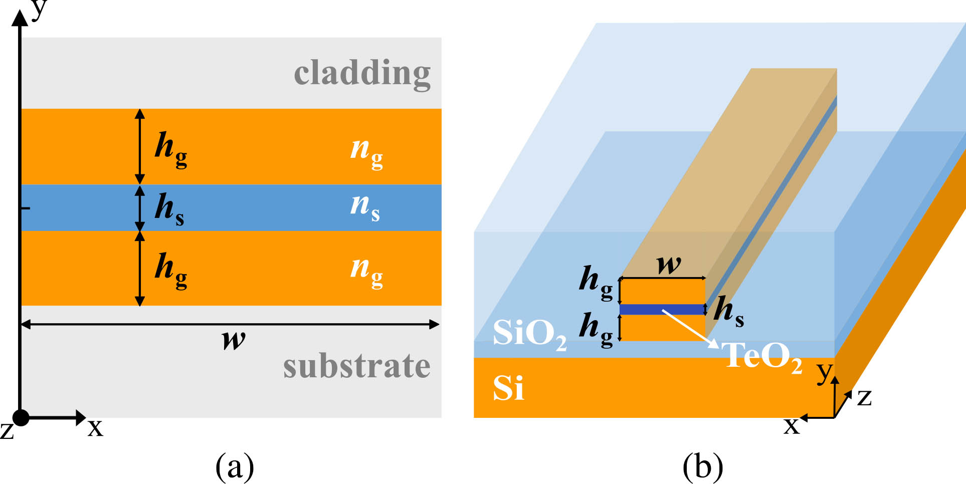
    Fig. 1. Structure of slot waveguide. (a) Two-dimensional schematic of horizontal slot waveguide; (b) three-dimensional schematic of horizontal slot waveguide.
    Distribution of normalized |E (x, y)| in slot waveguide with the Si guiding layer height hg = 200 nm, width w = 300 nm, and slot height hs = 40 nm. (a) TM mode profile at 1530 nm; (b) TM mode profile at 1480 nm; (c) TE mode profile at 1530 nm; (d) TE mode profile at 1480 nm. The white arrows represent the directions and amplitudes of the electric field in the xy plane.
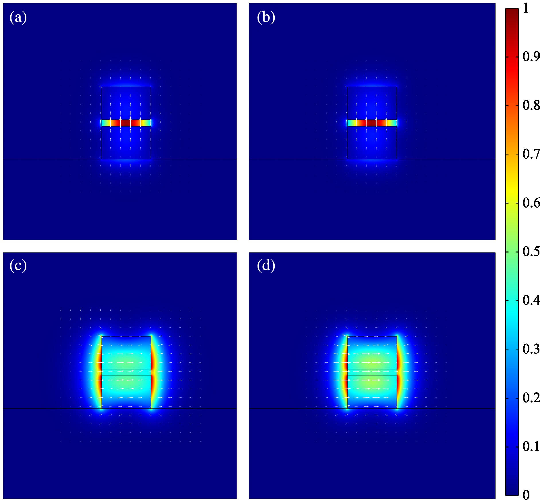
    Fig. 2. Distribution of normalized |E (x, y)| in slot waveguide with the Si guiding layer height hg = 200 nm, width w = 300 nm, and slot height hs = 40 nm. (a) TM mode profile at 1530 nm; (b) TM mode profile at 1480 nm; (c) TE mode profile at 1530 nm; (d) TE mode profile at 1480 nm. The white arrows represent the directions and amplitudes of the electric field in the xy plane.
    Simulation results for varying hs from 10 to 120 nm. (a) Effective refractive indices neff of the TM/TE mode at 1530 nm and 1480 nm; (b) confinement factors Γs of the TM/TE mode at 1530 nm and 1480 nm; (c) normalized power density Inorm of the TM/TE mode at 1530 nm and 1480 nm.
    Fig. 3. Simulation results for varying hs from 10 to 120 nm. (a) Effective refractive indices neff of the TM/TE mode at 1530 nm and 1480 nm; (b) confinement factors Γs of the TM/TE mode at 1530 nm and 1480 nm; (c) normalized power density Inorm of the TM/TE mode at 1530 nm and 1480 nm.
    Optimization of width and height of the Si layer with a 40 nm thick slot. (a) Field confinement factors Γs as a function of single silicon layer height hg and waveguide width w. (b) Normalized power density Inorm as a function of single silicon layer height hg and waveguide width w. The white dashed lines in (a) and (b) are the boundaries of the neff (TM) > neff (TE) condition; only the domains below these lines are valid. The white dots in (a) and (b) denote Γs = 29.17% and Inorm = 24.31 µm−2, respectively, at the positions of hg = 200 nm and w = 300 nm.
    Fig. 4. Optimization of width and height of the Si layer with a 40 nm thick slot. (a) Field confinement factors Γs as a function of single silicon layer height hg and waveguide width w. (b) Normalized power density Inorm as a function of single silicon layer height hg and waveguide width w. The white dashed lines in (a) and (b) are the boundaries of the neff (TM) > neff (TE) condition; only the domains below these lines are valid. The white dots in (a) and (b) denote Γs = 29.17% and Inorm = 24.31 µm−2, respectively, at the positions of hg = 200 nm and w = 300 nm.
    Energy-level transitions for the Er3+-doped four-level system (pumped by 1480 nm).
    Fig. 5. Energy-level transitions for the Er3+-doped four-level system (pumped by 1480 nm).
    Simulated gain characteristics of the designed slot waveguide amplifier. (a) Gain versus propagation distance for different pump powers. (b) Gain versus pump power for different amplifier lengths. For both situations, the signal power is assumed to be 0.01 mW.
    Fig. 6. Simulated gain characteristics of the designed slot waveguide amplifier. (a) Gain versus propagation distance for different pump powers. (b) Gain versus pump power for different amplifier lengths. For both situations, the signal power is assumed to be 0.01 mW.
    MaterialIndex at 1530 nmIndex at 1480 nm
    Si3.4783.482
    SiO21.4441.451
    TeO2:Er3+2.062.07
    Table 1. Refractive Indices Used in Simulation[22,23]
    ParameterFull nameValue
    NErErbium ion density2.2×1026m3
    σ12(νp)Absorption cross section at 1480 nm3.0×1024m2
    σ21(νp)Emission cross section at 1480 nm0.4×1024m2
    σ24(νp)Excited-state absorption cross section0.85×1025m2
    σ12(νs)Absorption cross section at 1530 nm3.5×1024m2
    σ21(νs)Emission cross section at 1530 nm4.4×1024m2
    A21Spontaneous emission rate of N22×103s1
    A32Spontaneous emission rate of N32.5×104s1
    A43Spontaneous emission rate of N4107s1
    CupUp-conversion coefficient2.7×1024m3·s1
    C14Cross-relaxation coefficient1.0×1023m3·s1
    LpPropagation loss of the pump laser1 dB/cm
    LsPropagation loss of the signal laser1 dB/cm
    Table 2. Parameter Values of TeO2:Er3+ Rate Equation Model[11,23]
    Ning Wei, Xiaobo Li, Jiajing He, Yongtao Fan, Yaping Dan, Jun Wang. Design of an optical slot waveguide amplifier based on Er3+-doped tellurite glass[J]. Chinese Optics Letters, 2023, 21(1): 011404
    Download Citation