• Chinese Optics Letters
  • Vol. 21, Issue 1, 011404 (2023)
Ning Wei1、2, Xiaobo Li1、2, Jiajing He1、2, Yongtao Fan1、2, Yaping Dan3, and Jun Wang1、2、4、5、*
Author Affiliations
  • 1Laboratory of Micro-Nano Optoelectronic Materials and Devices, Key Laboratory of Materials for High-Power Laser, Shanghai Institute of Optics and Fine Mechanics, Chinese Academy of Sciences, Shanghai 201800, China
  • 2Center of Materials Science and Optoelectronics Engineering, University of Chinese Academy of Sciences, Beijing 100049, China
  • 3University of Michigan-Shanghai Jiao Tong University Joint Institute, Shanghai Jiao Tong University, Shanghai 200240, China
  • 4CAS Center for Excellence in Ultra-intense Laser Science (CEULS), Shanghai 201800, China
  • 5State Key Laboratory of High Field Laser Physics, Shanghai Institute of Optics and Fine Mechanics, Chinese Academy of Sciences, Shanghai 201800, China
  • show less
    DOI: 10.3788/COL202321.011404 Cite this Article Set citation alerts
    Ning Wei, Xiaobo Li, Jiajing He, Yongtao Fan, Yaping Dan, Jun Wang. Design of an optical slot waveguide amplifier based on Er3+-doped tellurite glass[J]. Chinese Optics Letters, 2023, 21(1): 011404 Copy Citation Text show less

    Abstract

    The idea of a slot waveguide amplifier based on erbium-doped tellurite glass is first theoretically discussed in this work. Choosing the horizontal slot for low propagation loss, the TM mode profile compressed in the insertion layer was simulated, and the gain characteristics of the slot waveguide amplifier were calculated. Combining the capacity to confine light locally and the merits of tellurite glass as an emission host, this optimized amplifier shows enhanced interactions between the electric field and erbium ions and achieves a net gain of 15.21 dB for the 0.01 mW input light at 1530 nm, implying great promise of a high-performance device.

    1. Introduction

    Enabling the construction of complex optoelectronic systems in a reliable and cost-effective way, the potential of photonic integrated circuits (PICs) is now explored in many applications, such as optical communication[1,2], computing[3], sensing[4], and detecting[5]. There has been substantial progress achieved in recent years, however, transmission loss resulting from absorption, reflection, diffraction, scattering, or coupling efficiency remains a key challenge to improve the functionalities of integrated devices[68]. Limited by the fabrication technologies as well as material platforms, the attenuation of light energy at the interface is inevitable and not negligible, which should be compensated by optical amplification to ensure adequate power efficiency, signal noise ratio, or quality factor.

    Inspired by the great success of erbium-doped fiber amplifiers (EDFAs) in optical telecommunication, erbium-doped waveguide amplifiers (EDWAs) have attracted much attention in decades[9]. Compared to semiconductor optical amplifiers (SOAs) based on electron–hole pairs recombination in III–V semiconductors, EDWAs can offer longer excited-state lifetime, simpler structure, lower noise, broader bandwidth, and thermally stabler optical gain, allowing for high-speed amplification[9,10]. Despite the fact that Er ions interactions and clustering effects constrain the dopant concentration, highly Er3+-doped active materials are still sought to accomplish greater maximum gain, which makes waveguide amplifiers more competitive. Hence, significant investigations on host materials, co-dopant addition proportion, and fabrication techniques of EDWAs have been conducted. Glass hosts exhibit broad smooth emission spectra of Er3+ and good thermal stability, more suitable to develop a broadband amplifier than crystal or polymer. Among all glass host matrices, tellurite glass offers a number of advantages because of its high-refractive-index enabling compact devices, wide emission bandwidth, large emission cross section, low cross-relaxation coefficient, lower phonon energy, relative independence of the 1550 nm Er lifetime on concentration, and high Er solubility, as has been demonstrated in fiber amplifiers[1115]. To combine the outstanding gain material with the mature silicon-on-insulator (SOI) platform for the realization of a practical EDWA, an Er-doped tellurite glass amplifier based on a silicon slot waveguide is proposed in our work.

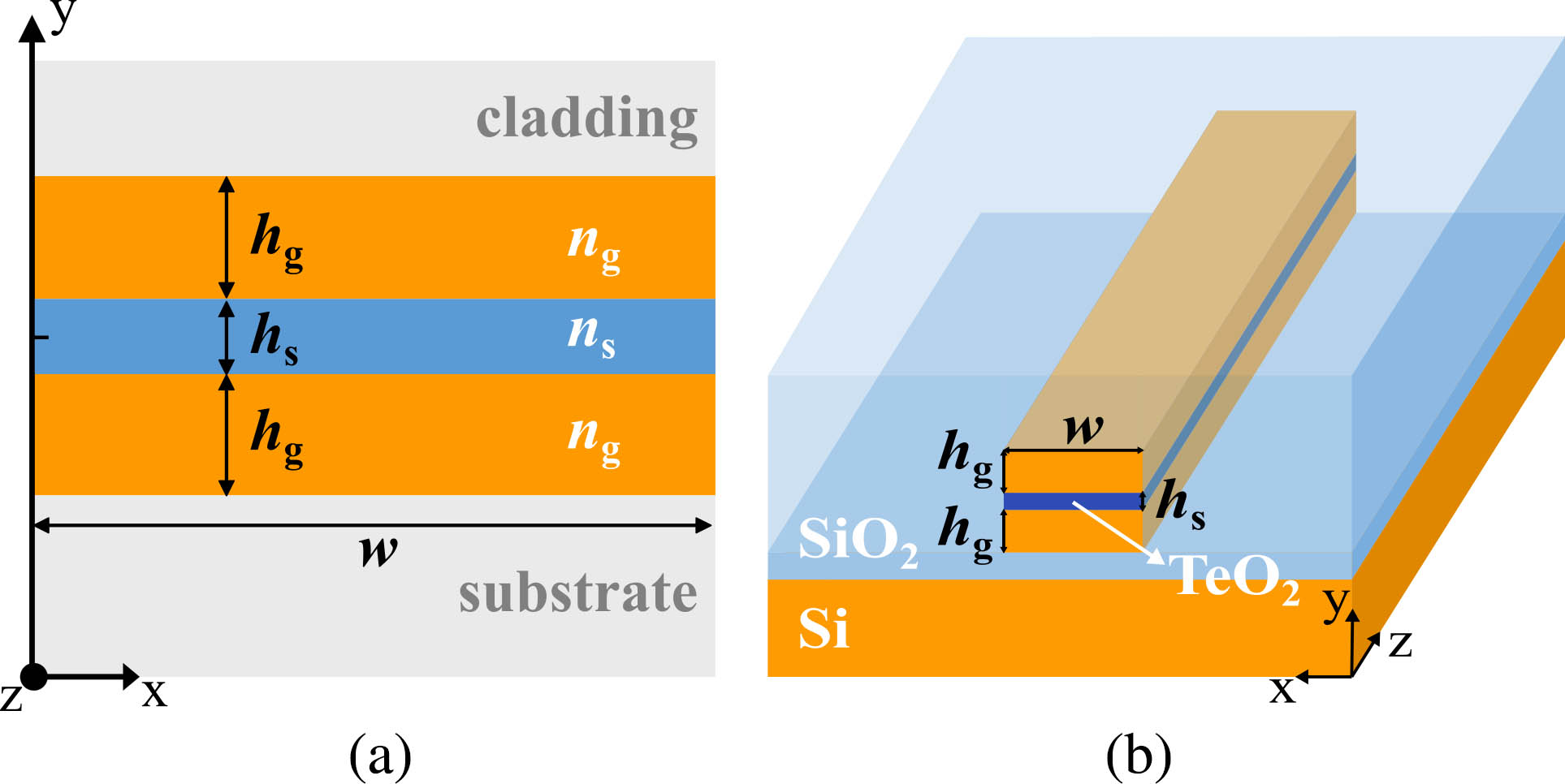
    Slot waveguides are of high interest in integrated optics owing to their ability to confine light strongly in a very thin low-refractive-index region. For this reason, they have shown great potential to produce high-performance integrated waveguide lasers and amplifiers[1619]. But, a vertical slot fabrication involves etching in a very narrow region, which can cause severe roughness in the waveguide sidewall in contrast to the precise and easy height control of the deposition layer in current micro/nanofabrication technologies; as a result, a horizontal slot is more favorable in the EDWA design for its lower propagation loss[20,21]. In this paper, a 40 nm thick horizontal slot of TeO2:Er3+ sandwiched by two high-index silicon strips is employed. Due to the electric displacement continuity boundary condition, the electric field of quasi-TM polarized light in the optically thinner medium will be enhanced by the factor of ng2/ns2 (Fig. 1). The Er-doped tellurite glass is filled into the slot as the core layer, and a four-level spectroscopic model pumped at 1480 nm is presented. By accurate optimization for the slot and calculation of gain characteristics, we demonstrate theoretically a 4 cm long EDWA with a net gain up to 15 dB for 1480 nm pump light, whose Er3+ concentration is 2.2×1026m3.

    Structure of slot waveguide. (a) Two-dimensional schematic of horizontal slot waveguide; (b) three-dimensional schematic of horizontal slot waveguide.

    Figure 1.Structure of slot waveguide. (a) Two-dimensional schematic of horizontal slot waveguide; (b) three-dimensional schematic of horizontal slot waveguide.

    2. Design of the Slot Waveguide

    Since active material exists in the slot region only, a waveguide in which pump and signal light is more concentrated in the low-refractive-index area is desired for higher energy availability. Also, a higher electric field intensity in the active material is needed for a stronger light–matter interaction. The trade-off of these two requirements implies that the structure of the slot waveguide used for amplification should be carefully designed, according to the mode distribution. In this work, the COMSOL software based on the finite element method (FEM) was used to simulate the modal distribution and optimize the waveguide structure. A two-dimensional model was built in the Wave Optics Module, coupled with the Electromagnetic Waves Frequency Domain (ewfd) interface, and studied by Mode Analysis solver. The schematics of the slot waveguide with horizontal sidewalls are displayed in Fig. 1. An image of the cross section of the sandwiched waveguide is shown in Fig. 1(a), and that in the 3D view is shown in Fig. 1(b). An Er-doped TeO2 glass layer with the height hs is inserted into the two silicon strip waveguides with the same height hg and width w as the gain medium. Outside the sandwich-structured silicon strip, the cladding and substrate materials are both silica. The three geometric parameters hs, hg, and w are focused on the following optimization.

    Considering the overlap between the signal and pump beam, the modal profile should be simulated at both λs (1530 nm) and λp (1480 nm). The refractive indices of waveguide materials chosen for simulation are shown in Table 1. The refractive index variation of TeO2:Er3+ owing to dopant concentration is neglected for its relatively small influence[22,24]. The modal profiles of electric field E(x,y) in the slot waveguide simulated at 1530 and 1480 nm are depicted in Fig. 2. From the simulation results, we can see that the horizontal slot waveguide is strongly polarization-sensitive: the enhanced electric field component of the y direction (Ey), which is perpendicular to the interface, causes the domination of the TM mode in the slot region. Thus, only the TM mode contributes to the amplification process.

    Distribution of normalized |E (x, y)| in slot waveguide with the Si guiding layer height hg = 200 nm, width w = 300 nm, and slot height hs = 40 nm. (a) TM mode profile at 1530 nm; (b) TM mode profile at 1480 nm; (c) TE mode profile at 1530 nm; (d) TE mode profile at 1480 nm. The white arrows represent the directions and amplitudes of the electric field in the xy plane.

    Figure 2.Distribution of normalized |E (x, y)| in slot waveguide with the Si guiding layer height hg = 200 nm, width w = 300 nm, and slot height hs = 40 nm. (a) TM mode profile at 1530 nm; (b) TM mode profile at 1480 nm; (c) TE mode profile at 1530 nm; (d) TE mode profile at 1480 nm. The white arrows represent the directions and amplitudes of the electric field in the xy plane.

    MaterialIndex at 1530 nmIndex at 1480 nm
    Si3.4783.482
    SiO21.4441.451
    TeO2:Er3+2.062.07

    Table 1. Refractive Indices Used in Simulation[22,23]

    To coordinate the two requirements in a more quantitative way, we define two figures of merit as follows: the light field confinement factor (Γs) in the slot region Γs=slot|E(x,y)|2dxdytotal|E(x,y)|2dxdy,and the normalized power density (Inorm)[25,26]Inorm=Γshsw.Γs represents the percentage of light energy transmitting in the slot, the part really utilized during the amplification process. Although a larger Γs is preferred, the high-energy proportion in the gain medium does not actually mean a strong light intensity, which directly determines rate of stimulated absorption or emission. To obtain the highest gain amplification, therefore, we should optimize the structure of the slot waveguide, taking both Γs and Inorm into account.

    As a prominent factor of slot waveguide functionality, the value of slot height hs is chosen first, then sweeping parameters of hg and w simultaneously to find the optimal variables relevant to specific hs. Before optimization, we assumed the hg=200nm and w=300nm, two moderate values acquired from previous articles[27,28]. The dependences of the effective refractive index (neff), Γs, and Inorm on hs are simulated at 1530 nm and 1480 nm under the presumption, as shown in Fig. 3. Because a high neff usually means a high-energy proportion of the corresponding mode, the relationship neff(TM)>neff(TE) is always requested throughout the design process. Apparently, from Fig. 3(a), the slot guiding structure supports a higher confinement in the slot region for the TM mode than that for the TE mode. Both the pump and signal light are confined in the slot under TM mode, and their interaction with the Er ion is enhanced in the slot, which will be beneficial for achieving higher gain. But, it is noted that Γs and Inorm show distinct changes with the increasing hs in Figs. 3(b) and 3(c). As the height of the low-refractive-index region rises, more light energy flows into the slot; but, the average power density reduces in the increasing area. For maximizing the light–matter interaction and minimizing the energy waste, therefore, a modest value hs=40nm is set in our EDWA design to reach a compromise; since a proper value ranges from 20 to 60 nm, where the curves in Figs. 3(b) and 3(c) change from the maximum to half.

    Simulation results for varying hs from 10 to 120 nm. (a) Effective refractive indices neff of the TM/TE mode at 1530 nm and 1480 nm; (b) confinement factors Γs of the TM/TE mode at 1530 nm and 1480 nm; (c) normalized power density Inorm of the TM/TE mode at 1530 nm and 1480 nm.

    Figure 3.Simulation results for varying hs from 10 to 120 nm. (a) Effective refractive indices neff of the TM/TE mode at 1530 nm and 1480 nm; (b) confinement factors Γs of the TM/TE mode at 1530 nm and 1480 nm; (c) normalized power density Inorm of the TM/TE mode at 1530 nm and 1480 nm.

    The silicon layer height hg and width w also need a trade-off between the two figures of merit. The relationships of Γs with the two parameters are illustrated in Fig. 4(a). It is revealed that Γs increases monotonically with w, but there is a maximum along with a heightening hg. The explanation of this phenomenon is that a wide w can alleviate the mode leakage in the Si(TeO2)-SiO2 interface, allowing more optical power to be accommodated in the waveguide; naturally, for the constant ratio of slot area to the waveguide’s, Γs will keep increasing when widening w. However, an excessive w in practice will lead to a proportional loss in the slot waveguide. Besides, the TE mode will gradually turn dominant like the eigenmode in a planar waveguide as the waveguide becomes flatter, which causes the w to be correctly selected. A similar alleviation of light leaking happens as well when increasing hg moderately, since the two strips with low height cannot confine the light in the slot and silicon layer well. But, continuing to increase the hg causes the reduction of the ratio of slot area to the whole cross section, and higher portions of light spread over the silicon strip. So, Γs tends to saturate and even decrease. In Fig. 4(b), Inorm is inversely related to w, while the change from hg resembles Γs’s. According to above results, w is appropriately determined to be 300 nm, and the corresponding optimal hg is 200 nm, showing that our prior assumption is reasonable.

    Optimization of width and height of the Si layer with a 40 nm thick slot. (a) Field confinement factors Γs as a function of single silicon layer height hg and waveguide width w. (b) Normalized power density Inorm as a function of single silicon layer height hg and waveguide width w. The white dashed lines in (a) and (b) are the boundaries of the neff (TM) > neff (TE) condition; only the domains below these lines are valid. The white dots in (a) and (b) denote Γs = 29.17% and Inorm = 24.31 µm−2, respectively, at the positions of hg = 200 nm and w = 300 nm.

    Figure 4.Optimization of width and height of the Si layer with a 40 nm thick slot. (a) Field confinement factors Γs as a function of single silicon layer height hg and waveguide width w. (b) Normalized power density Inorm as a function of single silicon layer height hg and waveguide width w. The white dashed lines in (a) and (b) are the boundaries of the neff (TM) > neff (TE) condition; only the domains below these lines are valid. The white dots in (a) and (b) denote Γs = 29.17% and Inorm = 24.31 µm−2, respectively, at the positions of hg = 200 nm and w = 300 nm.

    3. Gain Characteristics of Slot Waveguide Amplifier

    Supported by the optimization of the waveguide, the Er-doped low-refractive-index material is filled into the slot waveguide, and the potential gain of the slot waveguide amplifier is investigated. The gain characteristic analysis is based on the Er3+-doped four-level model, as shown in Fig. 5, and pumping at 1480 nm was chosen owing to the excessive absorption in the silicon layers and high excited-state absorption (ESA) of Er at 980 nm[29]. To achieve a more accurate simulation, the cooperative up-conversion (Cup), cross relaxation (C14), and spontaneous emission (A43, A32, A21) are involved. The operational principle of the amplifier pumped at 1480 nm is as follows: the Er3+ ions in the ground state absorb the photons and then are excited from the ground I415/2 level to the higher Stark split sub-levels in I413/2. Due to thermal relaxation, the excited ions rapidly decay to the lower, metastable sub-levels of I413/2. When the pump power exceeds the threshold power, population inversion is built between I415/2 and I413/2. Then, the rate of stimulated emission at 1530 nm caused by signal light overtakes the opposite stimulated absorption process, so the device realizes the light amplification. Here, the amplified spontaneous emission (ASE) was neglected. Combined with the ion interactions induced energy-level transitions, the simplified versions of the rate equations can be expressed by dN1dt=(W12+R12)N1+(W21+R21+A21)N2+CupN22C14N1N4,dN2dt=(W12+R12)N1(W21+R21+A21+R24)N2+A32N32(CupN22C14N1N4),dN3dt=A32N3+A43N4,dN4dt=R24N2A43N4+CupN22C14N1N4,NEr=N1+N2+N3+N4,where N1, N2, N3, and N4 are defined as the concentrations of Er3+ in the I415/2, I413/2, I411/2, and I49/2 energy states, respectively. NEr is the total Er3+ ion concentration. Supposing all Er3+ ions are uniformly doped and optically sensitized, the rate equations are analyzed under steady-state conditions of the population densities and solved using the method of overlap integral and an iteration method coupled with the propagation equations of the signal and the pump power, described by dPsdz=Γs[σ21(νs)N2σ12(νs)N1]PsαsPs,dPpdz=Γp[σ21(νp)N2σ24(νp)N2σ12(νp)N1]PpαsPp.

    Energy-level transitions for the Er3+-doped four-level system (pumped by 1480 nm).

    Figure 5.Energy-level transitions for the Er3+-doped four-level system (pumped by 1480 nm).

    The meanings and the values of the relevant parameters are shown in Table 2. Because it is difficult to test accurately all the parameters of the active material used in the simulation, the values in Table 2 are mainly accumulated from recent researches[11,29]. The 2.2×1026m3 dopant concentration and the 1 dB/cm loss coefficients of horizontal slot waveguide are typical amounts related to the promising reactive co-sputtering deposition technology. The initial signal power is determined to be 0.01 mW during the whole analysis process, so the propagation equations can be worked out by MATLAB using the Runge–Kutta algorithm, thus obtaining the gain characteristics through the iterative solving strategy for two sets of equations (shown in Fig. 6).

    Simulated gain characteristics of the designed slot waveguide amplifier. (a) Gain versus propagation distance for different pump powers. (b) Gain versus pump power for different amplifier lengths. For both situations, the signal power is assumed to be 0.01 mW.

    Figure 6.Simulated gain characteristics of the designed slot waveguide amplifier. (a) Gain versus propagation distance for different pump powers. (b) Gain versus pump power for different amplifier lengths. For both situations, the signal power is assumed to be 0.01 mW.

    ParameterFull nameValue
    NErErbium ion density2.2×1026m3
    σ12(νp)Absorption cross section at 1480 nm3.0×1024m2
    σ21(νp)Emission cross section at 1480 nm0.4×1024m2
    σ24(νp)Excited-state absorption cross section0.85×1025m2
    σ12(νs)Absorption cross section at 1530 nm3.5×1024m2
    σ21(νs)Emission cross section at 1530 nm4.4×1024m2
    A21Spontaneous emission rate of N22×103s1
    A32Spontaneous emission rate of N32.5×104s1
    A43Spontaneous emission rate of N4107s1
    CupUp-conversion coefficient2.7×1024m3·s1
    C14Cross-relaxation coefficient1.0×1023m3·s1
    LpPropagation loss of the pump laser1 dB/cm
    LsPropagation loss of the signal laser1 dB/cm

    Table 2. Parameter Values of TeO2:Er3+ Rate Equation Model[11,23]

    To study the dynamics of the amplification process where the pump and signal light are input to a slot waveguide in the same direction, the change of signal power propagating in the amplifier along with pump light is shown in Fig. 6(a). As can be seen, the signal gain functions versus propagation length under 0.1, 1, and 10 mW pumping are similar: the signal power increases at first and then decreases continually, and the length shows an optimum value. The mechanism is that the gain and loss are two competitive processes in the signal light transmission, the former stemming from the stimulated emission and the latter from absorption and propagation loss in the waveguide. Therefore, population inversion is critical to steer the net effect, which depends on whether the pump power is high enough to resist various de-population processes of the I413/2 level (e.g., spontaneous emission, non-radiative transition, ESA, and ion–ion interactions). Because pump power is constantly consumed in the transmission along the waveguide, after the first amplification of the small signal and reaching the optimal length, the pump power becomes smaller than the threshold power, and the amplification turns off, leaving the loss governing the subsequent propagation. Usually a high pump power is needed to achieve a longer active area and greater output gain. For instance, the optimum length and saturation output power are positively correlated to the pump power of curves pumped by 0.1, 1, and 10 mW in Fig. 6(a). But, an extremely high pump power always causes a severe ion–ion interaction, and consequently the augmented energy transfer up-conversion and ESA will degrade the gain characteristics seriously and even result in a pure “negative gain,” just as in the lowest curve of Fig. 6(a). From above analysis, it is known that a too long amplifier and a too high pump power all harm the performance, so the impact of pump power on gain characteristics entails assessing for a practical application. In Fig. 6(b), the four gain functions versus pump power of different length amplifiers are nearly identical. Obviously, the optimal pump power and maximum gain increase along with the increased length, but it shows a lower threshold power for a shorter amplifier owing to the smaller accumulative propagation loss. The largest pump power our designed 2.2×1026m3-doped TeO2:Er3+ amplifier can endure is located at 20 mW approximately. Below the tipping point, the highest gains, which 1, 2, 3, and 4 cm long amplifiers can attain, are predicted to be 6.08, 10.49, 13.37, and 15.21 dB, respectively.

    4. Conclusions

    Waveguide amplifiers have always been significant components for integrated photonics. Unfortunately, the low concentration of rare earth ions doped in the host and the inadequate optimization of the waveguide structure have been the common bottleneck. In our work, the performance of the horizontal slot waveguide amplifier based on Er3+-doped tellurite glass is simulated and evaluated. The modal characteristics under TE and TM modes were described. The slot structure can support a higher TM mode confined in the slot region compared to the TE mode. Despite doping the Er ions in silicon waveguide material, filling the gain medium into the horizontal slot eases the fabrication process, which is promised to be produced by reactive co-sputtering deposition. When the slot waveguide had an optimal width of 300 nm, a silicon height of 200 nm, and a slot width of 40 nm, the light field confinement factor and normalized power density in the slot region for TM polarization were 0.2917 and 24.31μm2 at 1530 nm, respectively. A four-level spectroscopic model pumped at 1480 nm was presented. The rate equations and propagation equations were solved, and the gain characteristics of the slot waveguide amplifier were numerically simulated. The primary parameters were optimized. A net gain of 15.21 dB was achieved for the signal power of 0.01 mW at 1530 nm, pump power of 2 mW, Er3+ concentration of 2.2×1026m3, and waveguide length of 4 cm.

    References

    [1] K. Liu, H. Fan, Y. Huang, X. Duan, Q. Wang, X. Ren, Q. Wei, S. Cai. A pair of integrated optoelectronic transceiving chips for optical interconnects. Chin. Opt. Lett., 16, 091301(2018).

    [2] E. Agrell, M. Karlsson, A. R. Chraplyvy, D. J. Richardson, P. M. Krummrich, P. Winzer, K. Roberts, J. K. Fischer, S. J. Savory, B. J. Eggleton, M. Secondini, F. R. Kschischang, A. Lord, J. Prat, I. Tomkos, J. E. Bowers, S. Srinivasan, M. Brandt-Pearce, N. Gisin. Roadmap of optical communications. J. Opt., 18, 063002(2016).

    [3] W. Bogaerts, D. Pérez, J. Capmany, D. A. B. Miller, J. Poon, D. Englund, F. Morichetti, A. Melloni. Programmable photonic circuits. Nature, 586, 207(2020).

    [4] A. Hänsel, M. J. R. Heck. Opportunities for photonic integrated circuits in optical gas sensors. J. Phys. Photonics, 2, 12002(2020).

    [5] J. Fridlander, F. Sang, V. Rosborough, F. Gambini, S. T. Šuran-Brunelli, J. R. Chen, K. Numata, M. Stephen, L. A. Coldren, J. Klamkin. Dual laser indium phosphide photonic integrated circuit for integrated path differential absorption lidar. IEEE J. Sel. Top. Quantum Electron., 28, 6100208(2022).

    [6] A. Rahim, A. Hermans, B. Wohlfeil, D. Petousi, B. Kuyken, D. V. Thourhout, R. Baets. Taking silicon photonics modulators to a higher performance level: state-of-the-art and a review of new technologies. Adv. Photonics, 3, 024003(2021).

    [7] L. Lu, S. Zhao, L. Zhou, D. Li, Z. Li, M. Wang, X. Li, J. Chen. Non-blocking silicon optical switch based on electro-optic Mach-Zehnder interferometers. Opt. Express, 24, 9295(2016).

    [8] L. He, Ş. K. Özdemir, L. Yang. Whispering gallery microcavity lasers. Laser Photon. Rev., 7, 60(2012).

    [9] J. D. B. Bradley, M. Pollnau. Erbium-doped integrated waveguide amplifiers and lasers. Laser Photon. Rev., 5, 368(2010).

    [10] D. R. Zimmerman, L. H. Spiekman. Amplifiers for the masses: EDFA, EDWA, and SOA amplets for metro and access applications. J. Light. Technol., 22, 63(2004).

    [11] H. C. Frankis, H. M. Mbonde, D. B. Bonneville, C. Zhang, R. Mateman, A. Leinse, J. D. B. Bradley. Erbium-doped TeO2-coated Si3N4 waveguide amplifiers with 5 dB net gain. Photon. Res., 8, 127(2020).

    [12] J. S. Wang, E. M. Vogel, E. Snitzer. Tellurite glass: a new candidate for fiber devices. Opt. Mater., 3, 187(1994).

    [13] A. Mori, Y. Ohishi, S. Sudo. Erbium-doped tellurite glass fibre laser and amplifier. Electron. Lett., 33, 863(1997).

    [14] Y. Ohishi, A. Mori, M. Yamada, H. Ono, Y. Nishida, K. Oikawa. Gain characteristics of tellurite-based erbium-doped fiber amplifiers for 1.5-µm broadband amplification. Opt. Lett., 23, 274(1998).

    [15] S. Shen, A. Jha, X. Liu, M. Naftaly, K. Bindra, H. J. Bookey, A. K. Kar. Tellurite glasses for broadband amplifiers and integrated optics. J. Am. Ceram. Soc., 85, 1391(2002).

    [16] V. R. Almeida, Q. Xu, C. A. Barrios, M. Lipson. Guiding and confining light in void nanostructure. Opt. Lett., 29, 1209(2004).

    [17] J. T. Robinson, C. Manolatou, L. Chen, M. Lipson. Ultrasmall mode volumes in dielectric optical microcavities. Phys. Rev. Lett., 95, 143901(2005).

    [18] C. A. Barrios, M. Lipson. Electrically driven silicon resonant light emitting device based on slot-waveguide. Opt. Lett., 13, 10092(2005).

    [19] M. Galli, D. Gerace, A. Politi, M. Liscidini, M. Patrini, L. C. Andreani, A. Canino, M. Miritello, R. L. Savio, A. Irrera, F. Priolo. Direct evidence of light confinement and emission enhancement in active silicon-on-insulator slot waveguides. Appl. Phys. Lett., 89, 241114(2006).

    [20] R. Sun, P. Dong, N. Feng, C. Hong, J. Michel, M. Lipson, L. Kimerling. λ = 1550 nm horizontal single and multiple slot waveguides: optical transmission at λ = 1550 nm. Opt. Express, 15, 17967(2007).

    [21] A. Tengattini, D. Gandolfi, N. Prtljaga, A. Anopchenko, J. M. Ramirez, F. F. Lupi, Y. Berencen, D. Navarro-Urrios, P. Rivallin, K. Surana, B. Garrido, J.-M. Fedeli, L. Pavesi. Toward a 1.54 µm electrically driven erbium-doped silicon slot waveguide and optical amplifier. J. Light. Technol., 31, 391(2013).

    [22] V. A. G. Rivera, D. Manzani. Technological Advances in Tellurite Glasses: Properties, Processing, and Applications(2017).

    [23] M. Zhang, G. Hu, S. Zhang, D. Gao, Y. Sun, F. Wang. Gain characteristics of the hybrid slot waveguide amplifiers integrated with NPs-PMMA covalently linked nanocomposites. RSC Adv., 10, 11148(2020).

    [24] R. A. H. El-Mallawany. Tellurite Glasses Handbook: Physical Properties and Data(2016).

    [25] T. D. Visser, H. Blok, B. Demeulenaere, D. Lenstra. Confinement factors and gain in optical amplifiers. IEEE J. Quantum Electron., 33, 1763(1997).

    [26] N. Feng, J. Michel, L. C. Kimerling. Optical field concentration in low-index waveguides. IEEE J. Quantum Electron., 42, 883(2006).

    [27] P. Mullner, R. Hainberger. Structural optimization of silicon-on-insulator slot waveguides. IEEE Photon. Technol. Lett., 18, 2557(2006).

    [28] P. Sanchis, J. Blasco, A. Martinez, J. Marti. Design of silicon-based slot waveguide configurations for optimum nonlinear performance. J. Light. Technol., 25, 1298(2007).

    [29] Y. Hu, S. Jiang, G. Sorbello, T. Luo, Y. Ding, B. Hwang, J. Kim, H. Seo, N. Peyghambarian. Cooperative upconversion in a new high-Er-doped tellurite glass. Proc. SPIE, 4282, 57(2001).

    Ning Wei, Xiaobo Li, Jiajing He, Yongtao Fan, Yaping Dan, Jun Wang. Design of an optical slot waveguide amplifier based on Er3+-doped tellurite glass[J]. Chinese Optics Letters, 2023, 21(1): 011404
    Download Citation