
En-Ming You, Yiqin Chen, Jun Yi, Zhao-Dong Meng, Qian Chen, Song-Yuan Ding, Huigao Duan, Martin Moskovits, Zhong-Qun Tian. Nanobridged rhombic antennas supporting both dipolar and high-order plasmonic modes with spatially superimposed hotspots in the mid-infrared[J]. Opto-Electronic Advances, 2021, 4(12): 210076-1
- Opto-Electronic Advances
- Vol. 4, Issue 12, 210076-1 (2021)
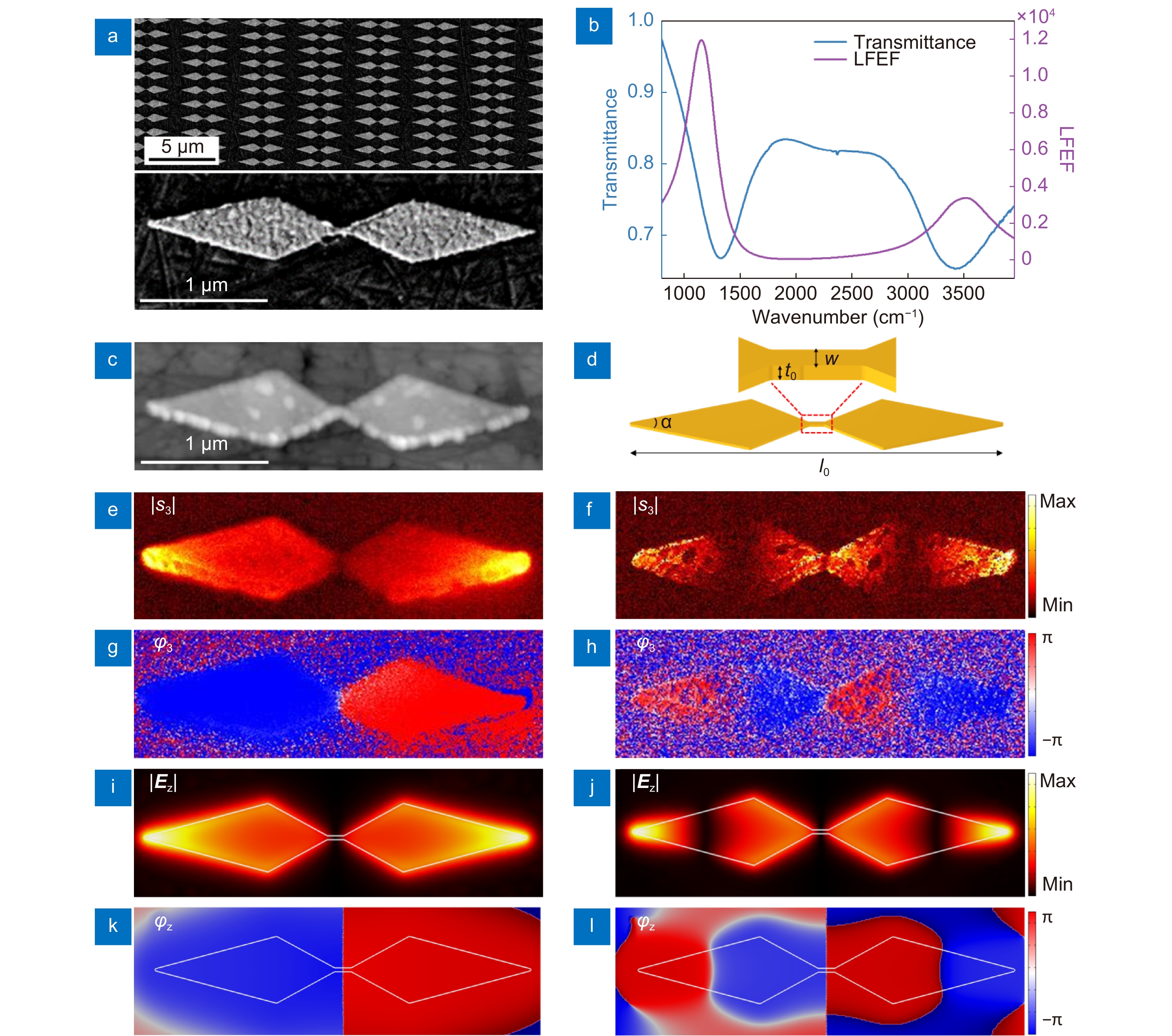
Fig. 1. (a ) Scanning electron microscopy (SEM) image of NBRA structures. (b ) Experimental transmittance of the NBRA array (blue curve) and simulated LFEF at the extremities of the structure (purple curve). (c ) AFM topography of a single NBRA structure. The scale bars are 1 μm. (d ) Sketch and parameters of the NBRA structure, consisting of two rhombic arms connected with each other by a nanobridge. The thickness (t 0) and total length (l 0) of NBRA are 30 nm and 2800 nm. The nanobridge is 30 nm in width and 130 nm in length. The radius of sharp tip of each arm is 10 nm and α is 30°. (e –h ) Measured near-field (e, f) amplitude and (g, h) phase of single NBRA structure at 1100 cm−1 and 2100 cm−1, respectively. (i –l ) Simulated |E φ z (k, l) of single NBRA structure at 1100 cm−1 and 2100 cm−1, respectively.
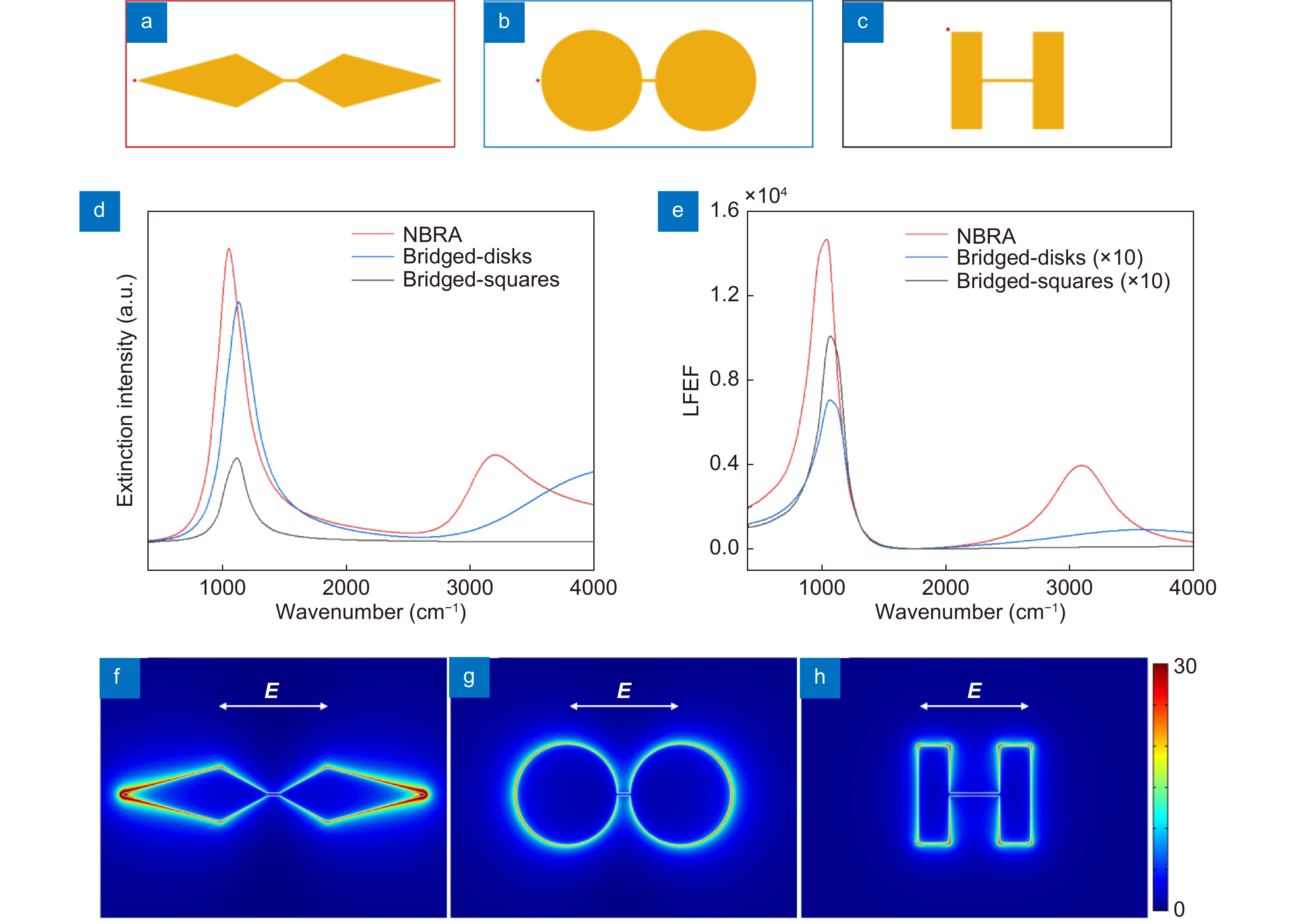
Fig. 2. The model of (a ) NBRA, (b ) nano-bridged disks and (c ) nano-bridged rectangles. All the structures are placed on the CaF2 substrate. The incident polarizations are along the long-axis of the nanobridge. The thickness and the width of the nanobridge are 30 nm for all three structures. The lengths of the nanobridges are 130 nm for the NBRA and the nanobridged-disks, and 500 nm for the nanobridged-rectangles. The total length of the NBRA is 3000 nm. The radius of the disks are 500 nm. The length and width of the rectangles are 962 nm and 308 nm, respectively. The red points in (a–c) are the positions where the LFEFs are evaluated. The LFEF was evaluated at the point 2 nm away from the structure along the long axis and 15 nm above the CaF2 substrate for the NBRA and the nanobridged-disks. While for the nanobridged-rectangles, the evaluating point is 2 nm away from the corner of the rectangle. (d ) The simulated extinction spectra and (e ) the LFEFs of all three structures. E-field distributions at the CTP resonance for (f ) the NBRA, (g ) the nanobridged-disks and (h ) the nanobridged-rectangles.
Fig. 3. (a ) Simulated extinction spectra of NBRA structure with different nanobridge width. (b –c ) Simulated mapping of |E z| of bonding dipolar plasmonic band (b) and bonding quadrupolar plasmonic band (c) of a single NBRA structure with a broken nanobridge and 4 nm gap size. (d –e ) Simulated mapping of |E z| at CTP band (d) and BDP band (e) with 370 nm nanobridge width.
Fig. 4. Nanobridge width-dependent (a ) resonant frequencies and (b ) intensities of CTP and BDP bands. The orange and blue circles are extracted from the simulated extinction spectra (Fig. 3(a)), while the points on the fitting curves are extracted from the spectra of
(Fig. S12, Supplementary information). Inset in (a): RLC circuit model of the NBRA structure. (c ) Nanobridge width-dependent ratio of
(blue curve in the top panel),
(purple curve in the top panel),
(blue curve in the bottom panel) and
(purple curve in the bottom panel). (d) Nanobridge width-dependent ratio of
(blue curve) and
(purple curve).
and
are the deterministic parameters for
.
Fig. 5. (a ) Experimental transmittance spectra (normalized) as a function of the length of the NBRAs. (b ) SEIRA spectra of PNTP on NBRAs with total lengths 2.22, 2.40, 2.57 and 2.90 μm in the range of the CTP band.
Fig. 6. (a ) SEM image of NBRA dimer. (b ) Experimental transmittance of a NBRA and its dimer with gap size 20 nm. (c ) AFM topography of a NBRA dimer. The scale bars in (a) and (c) are 1 μm. Measured near-field amplitude (d ) and phase (f ) of NBRA dimer at 1100 cm−1. Simulated mapping of |E h ) and φ z (j ) of NBRA dimer at 1100 cm−1. Measured near-field amplitude (e ) and phase (g ) of NBRA dimer at 2100 cm−1. Simulated mapping of |E i ) and φ z (k ) of NBRA dimer at 2100 cm−1.
Fig. 7. (a ) SEM of the cross section of the reflective substrate. A 200 nm gold film is sandwiched between a 1400 nm SiO2 spacer layer and the Si substrate. The scale bar is 1 μm. Inset: schematic of the NBRA dimer-on-reflector structure to integrate the waveguide-cavity coupling and nanogap coupling. (b ) Normalized LFEFs of CTP mode (blue curve) and BDP mode (orange curve) as a function of the thickness of the spacer layer. (c ) Simulated LFEFs of monomer, dimer and dimer with 1400 nm SiO2 spacer layer. (d ) SEIRA spectra of PNTP on NBRA dimer on transmitted substrate or on reflective substrate.
|
Table 1. Fitting parameters used in the RCL circuit model

Set citation alerts for the article
Please enter your email address
© Copyright 2018-2021 | Chinese Laser Press. All Rights Reserved 沪ICP备15018463号-20