
Carlos Pérez-Armenta, Alejandro Ortega-Moñux, José Manuel Luque-González, Robert Halir, Pedro J. Reyes-Iglesias, Jens Schmid, Pavel Cheben, Íñigo Molina-Fernández, J. Gonzalo Wangüemert-Pérez. Polarization-independent multimode interference coupler with anisotropy-engineered bricked metamaterial[J]. Photonics Research, 2022, 10(4): A57
- Photonics Research
- Vol. 10, Issue 4, A57 (2022)
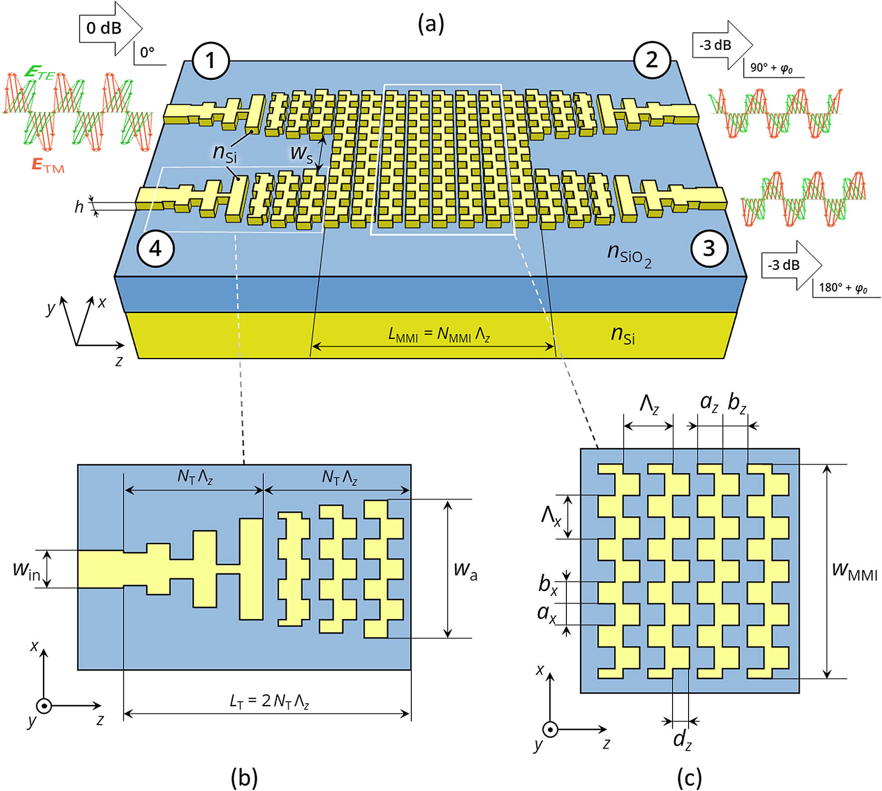
Fig. 1. (a) Schematic of the proposed polarization-insensitive 2 × 2 SiO 2
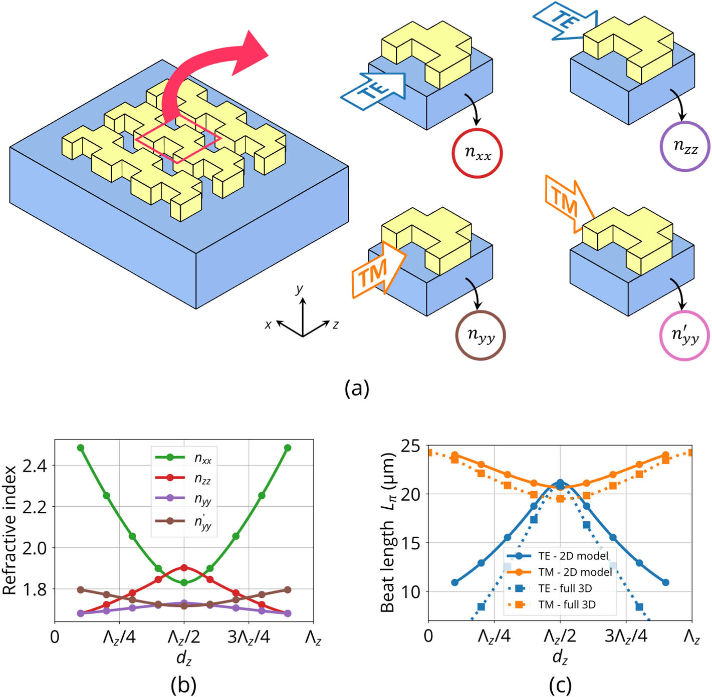
Fig. 2. (a) Procedure employed for modeling the bricked SWG. (b) Calculated refractive index components for a bricked SWG waveguide with h = 220 nm Λ x = 200 nm DC x = 50 % Λ z = 240 nm DC z = 50 % λ = 1.31 μm w MMI = 3 μm
Fig. 3. Design methodology used in this work, comprising two main stages: (a) design of the bricked SWG multimode waveguide and (b) optimization of the complete device using a 3D-FDTD simulator.
Fig. 4. Absolute value of the relative difference between TE and TM beat lengths | Δ L π ¯ | = | Δ L π / L π ¯ | Δ L π = L π ( TE ) − L π ( TM ) L π ¯ = ( L π ( TE ) + L π ( TM ) ) / 2 h = 220 nm DC z = DC x = 50 % Λ x = 200 nm λ = 1.31 μm ( d z , Λ z ) Δ L π ¯ = 0 Λ z = 240 nm d z = Λ z / 2
Fig. 5. Beat length as a function of wavelength obtained from 3D Floquet–Bloch simulations of the (bricked) SWG waveguide. Solid lines correspond to d z = 0 d z = 0.48 Λ z w MMI = 3 μm h = 220 nm Λ x = 200 nm DC x = 50 % Λ z = 220 nm DC z = 50 %
Fig. 6. Final design performance of the optimized polarization-independent 2 × 2
Fig. 7. Dependence of the bandwidth and center wavelength of the MMI on fabrication error δ | IB | δ
Fig. 8. Calculation of | Δ L π ¯ | 4 for different transversal periods Λ x DC = DC x = DC z λ = 1310 nm | Δ L π | = 0 Λ x > 200 nm DC ≠ 50 % | Δ L π ¯ |
|
Table 1. Optimized Design Parameters of Polarization Insensitive 2 × 2
|
Table 2. Comparison of Our Device with Other State-of-the-Art Polarization-Insensitive SOI-based MMI Couplers

Set citation alerts for the article
Please enter your email address
© Copyright 2018-2021 | Chinese Laser Press. All Rights Reserved 沪ICP备15018463号-20