• Journal of Infrared and Millimeter Waves
  • Vol. 40, Issue 5, 680 (2021)
Hao-Chen TONG1, Shu-Min TANG1, Shu-Ming YE1, Xiao-xiao Duan1, Xiao-Nan LI1, Ji-Yang XIE1, Lu-Ran ZHANG1, Jie YANG1, Feng QIU1, Rong-Fei WANG1、*, Xiao-Ming WEN2, Yu Yang1, Hao-Yang CUI3, and Chong WANG1、**
Author Affiliations
  • 1National Center for International Research on Photoelectric and Energy Materials,School of Materials and Energy,Yunnan University,Kunming 650091,China
  • 2Centre for Translational Atomaterials,Swinburne University of Technology,Hawthorn3122,Australia
  • 3College of Electronic and Information Engineering,Shanghai University of Electric Power,Shanghai 200090,China.
  • show less
    DOI: 10.11972/j.issn.1001-9014.2021.05.015 Cite this Article
    Hao-Chen TONG, Shu-Min TANG, Shu-Ming YE, Xiao-xiao Duan, Xiao-Nan LI, Ji-Yang XIE, Lu-Ran ZHANG, Jie YANG, Feng QIU, Rong-Fei WANG, Xiao-Ming WEN, Yu Yang, Hao-Yang CUI, Chong WANG. Effective enhancement of the photoluminescence from the Si+/Ni+ ions co-implanted SOI by directly constructing the nanodisk photonic crystals[J]. Journal of Infrared and Millimeter Waves, 2021, 40(5): 680 Copy Citation Text show less
    Preparation process of Au film photonic crystal array.
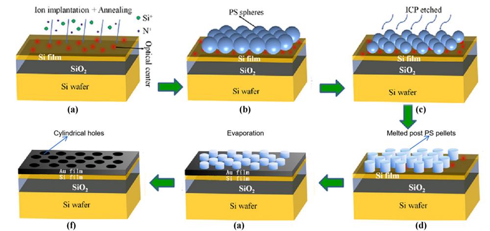
    Fig. 1. Preparation process of Au film photonic crystal array.
    (a)Simulation of electric field strength of Au film without photonic crystal structure(b)Simulation of electric field strength of Au film with photonic crystal structure(c)SEM characterization of Au film photonic crystal structure sample.
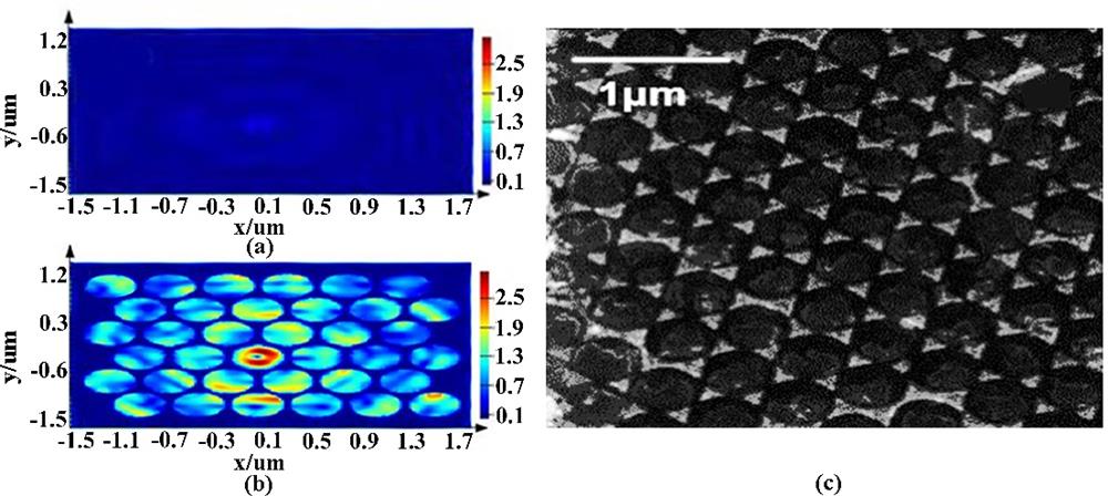
    Fig. 2. (a)Simulation of electric field strength of Au film without photonic crystal structure(b)Simulation of electric field strength of Au film with photonic crystal structure(c)SEM characterization of Au film photonic crystal structure sample.
    PL spectra and Puercell factor of Si + / Ni + ion co-implanted SOI nanodisk Au film sample and the uncovered sample as well as the simulated sample.
    Fig. 3. PL spectra and Puercell factor of Si + / Ni + ion co-implanted SOI nanodisk Au film sample and the uncovered sample as well as the simulated sample.
    The photonic band gap of the sample with the Au nanodisk-array photonic crystals which simulated by the FDTD software. The 3.6×10¹⁴-3.7×10¹⁴ Hz(810~830 nm)range corresponding to the solid black line is the photonic forbidden band,and the black dotted line corresponds to the luminous peak at 3.5×10¹⁴ Hz(857nm).
    Fig. 4. The photonic band gap of the sample with the Au nanodisk-array photonic crystals which simulated by the FDTD software. The 3.6×10¹⁴-3.7×10¹⁴ Hz(810~830 nm)range corresponding to the solid black line is the photonic forbidden band,and the black dotted line corresponds to the luminous peak at 3.5×10¹⁴ Hz(857nm).
    Hao-Chen TONG, Shu-Min TANG, Shu-Ming YE, Xiao-xiao Duan, Xiao-Nan LI, Ji-Yang XIE, Lu-Ran ZHANG, Jie YANG, Feng QIU, Rong-Fei WANG, Xiao-Ming WEN, Yu Yang, Hao-Yang CUI, Chong WANG. Effective enhancement of the photoluminescence from the Si+/Ni+ ions co-implanted SOI by directly constructing the nanodisk photonic crystals[J]. Journal of Infrared and Millimeter Waves, 2021, 40(5): 680
    Download Citation