
Chunhui Lu, Hongwen Xuan, Yixuan Zhou, Xinlong Xu, Qiyi Zhao, Jintao Bai. Saturable and reverse saturable absorption in molybdenum disulfide dispersion and film by defect engineering[J]. Photonics Research, 2020, 8(9): 1512
- Photonics Research
- Vol. 8, Issue 9, 1512 (2020)
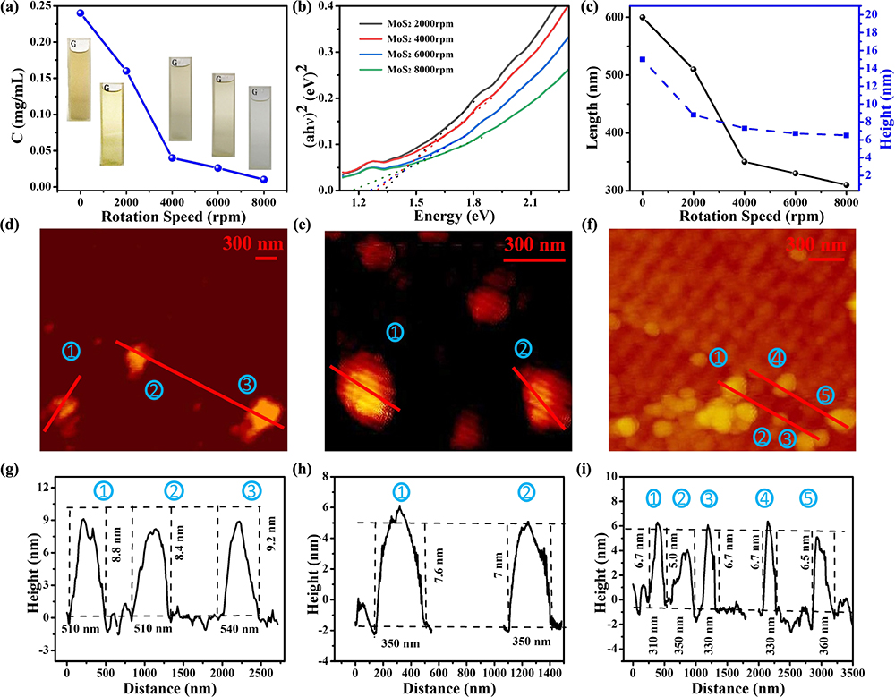
Fig. 1. (a) Concentrations of MoS 2 MoS 2 MoS 2 MoS 2 MoS 2 MoS 2
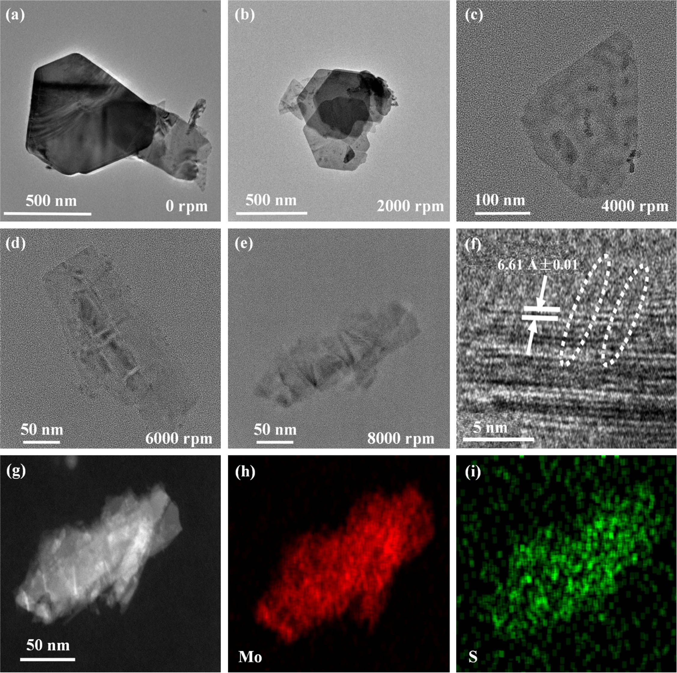
Fig. 2. Representative TEM images of MoS 2 MoS 2 MoS 2
Fig. 3. (a) High-resolution XPS spectra of MoS 2 MoS 2 MoS 2 E 2 g 1 A 1 g MoS 2 MoS 2
Fig. 4. Open-aperture Z-scan results of MoS 2 MoS 2
Fig. 5. (a) Calculated results of α 0 β eff Im χ ( 3 ) MoS 2 α 0 β eff Im χ ( 3 )
Fig. 6. Band structure and DOS results for monolayer MoS 2
Fig. 7. (a) Three-energy-level model of few or few-defect MoS 2 MoS 2 MoS 2 MoS 2 MoS 2
|
Table 1. Parameters of

Set citation alerts for the article
Please enter your email address
© Copyright 2018-2021 | Chinese Laser Press. All Rights Reserved 沪ICP备15018463号-20