Abstract
Understanding and controlling defect in two-dimensional materials is important for both linear and nonlinear optoelectronic devices, especially in terms of tuning nonlinear optical absorption. Taking advantage of an atomic defect formed easily by smaller size, molybdenum disulfide nanosheet is prepared successfully with a different size by gradient centrifugation. Interestingly, size-dependent sulfur vacancies are observed by high-resolution X-ray photoelectron spectroscopy, atomic force microscopy, and transmission electron microscopy. The defect effect on nonlinear absorption is investigated by Z-scan measurement at the wavelength of 800 nm. The results suggest the transition from saturable absorption to reverse saturable absorption can be observed in both dispersions and films. First principle calculations suggest that sulfur vacancies act as the trap state to capture the excited electrons. Moreover, an energy-level model with the trap state is put forward to explain the role of the sulfur vacancy defect in nonlinear optical absorption. The results suggest that saturable absorption and reverse saturable absorption originate from the competition between the excited, defect state and ground state absorption. Our finding provides a way to tune the nonlinear optical performance of optoelectronic devices by defect engineering.1. INTRODUCTION
Unavoidable defects in the growth process of two-dimensional (2D) materials can dramatically affect the performance of the corresponding device. Defect-associated nonradiative recombination will lead to low quantum efficiency () [1], and structure defects will result in lower carrier mobility [2]. Defects can also be a source of merit; for instance, photoluminescence enhancement induced by sulfur (S) vacancy [3] and oxygen bonding at the defect sites [4] in monolayer molybdenum disulfide () and catalytic efficiency in hydrogen evolution reaction improved by S vacancies [5] at edge defects [6]. However, the contribution of these defects to the nonlinear optical (NLO) properties, such as saturable absorption (SA) and reverse saturable absorption (RSA), is not completely clear so far. Recently, different defect types, including effective two-photon absorption (TPA) from zinc (Zn) vacancy [7], tunable NLO absorption derived from the concentration of manganese doping [8], and enhanced modulation depth [9] from localized defect states at grain boundaries, have been introduced to improve the performance of nonlinear photonic devices. Actually, these defects act as different trap centers to capture electrons [10], holes [11], or excitons [12,13], which make it crucial to confirm the type of defect-induced localized states in 2D materials.
is a typical 2D material to design linear optoelectronic devices due to its excellent optical and electronic properties, including high current on/off ratio (), high electron mobility () [14], strong catalytic activity [15], and photoluminescence [16,17]. Importantly, a size-dependent few-layer can be achieved easily using ultrasonic exfoliation [18] combined with the gradient centrifugation method [19]. On the other hand, nonlinear photonic applications including -switching [20], mode-locking [21,22], and an optical limiter [23] have also been designed based on SA and RSA behavior. For example, and graphene were reported with stronger SA [24] than those of and , while BN exhibited a strong RSA effect [25]. SA and RSA can be interpreted as a transmission increasing and decreasing according to pump intensity, respectively. It is determined by a smaller absorption cross section in excited state compared with that in ground state for SA [20,26]. On the other hand, RSA occurs due to larger absorption cross section in excited state compared with that in ground state. Including SA and RSA, some defects can be introduced to improve optical and electronic properties in material. For instance, the defect level of bulk can be tuned from 1.08 to 0.08 eV [27] by S vacancies. The S vacancies can easily transform into an n-type conductor, whereas the Mo vacancies can be used to transform into a p-type conductor [28]. Particularly, these atomic defects are easily formed in small nanosheets compared to those in large nanosheets [29]. Interestingly, the changeover from SA to RSA has been observed in nanosheet dispersions with size using a picosecond laser [30], which is caused by certain edge defect. However, the defect type-size relationship is yet to be identified as well as its related mechanisms in NLO properties. In addition, the reported nonlinear responses are based on liquid environments, and thus it is hard to avoid thermally induced nonlinear scattering [31]. A femtosecond laser source can avoid this condition due to the slow formation of bubbles from the ultrashort pulse laser [32]. It is also easy to solve the problem and design nonlinear optics-based devices by preparing films [33].
In this work, we first present an effective method to introduce S vacancies in by adjusting the nanosheet size. Different nanosheet sizes are obtained through liquid-phase exfoliation by controlling the centrifugation speed, and films with different sizes are fabricated by the vacuum filtration technique. The successful size-separation is identified by atomic force microscopy (AFM) and transmission electron microscopy (TEM). The size-dependent S vacancies are confirmed by Raman spectroscopy and high-resolution X-ray photoelectron spectroscopy (XPS). The influence of S vacancy concentration on NLO properties is studied by a typical Z-scan setup at 800 nm. The changeover from SA to RSA is observed both in films and dispersions. Combined with the S vacancy defect state, which is confirmed by first principle calculations, an energy-level model is carried out based on S vacancy concentration. SA and RSA are strongly related to ground state, excited state, and defect state absorption. This work provides a method to tune nonlinear photonic devices by controlling the defects.
Sign up for Photonics Research TOC. Get the latest issue of Photonics Research delivered right to you!Sign up now
2. RESULTS AND DISCUSSION
A. Methods: Nanosheet Dispersion and Film Preparation
A green ethanol-based solvent exfoliation process was used to prepare few-layer nanosheets [34]. Initially, we chose 40% ethanol mixed with deionized water for 0.9 g in a 300 mL mixed solution. We settled the parameters with 700 W for 3 h using the supersonic machine (Qsonica Q700) to prepare the dispersion. After that, the nanosheet supernatant was acquired with a centrifuge (Centurion Scientific K241) by controlling the rotation speeds with 2000 rpm, 4000 rpm, 6000 rpm, and 8000 rpm for 15 min to remove large nanoparticles. To obtain a larger nanosheet, ultrasonic exfoliation with 70 W for 3 h was used and then let the acquired dispersion stand two weeks with 0 rpm. Subsequently, we can prepare the films with almost the same thickness by controlling filtration volume using the vacuum filtration technique.
B. Characterization of Dispersions and Films
The nanosheet was successfully exfoliated from optical images of dispersion and presented in Fig. 1(a). In addition, concentration was measured from 0.01 to 0.24 mg/mL. To investigate the relationship between the size and optical bandgap, a Tauc plot derived from UV–Vis spectra of dispersions with a different centrifugation speed is given in Fig. 1(b). The result shows that the bandgap of dispersions ranged from 1.36 to 1.27 eV with increased centrifugation speed. The size-dependent bandgap is supposed to be induced by S and Mo atom vacancies [2,35].
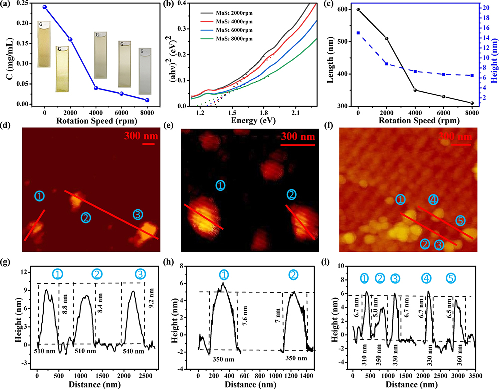
Figure 1.(a) Concentrations of dispersion at different rotation speeds with related optical images inserted. (b) Tauc plot of dispersions. (c) Size and height of dispersions at different rotation speeds. (d), (g) AFM image and height profile of at 2000 rpm. (e), (h) AFM image and height profile of at 4000 rpm. (f), (i) AFM image and height profile of at 6000 rpm. The number indicates the different nanosheet.
To further confirm the successful size-separation of , the dispersions were dropped respectively on glass substrate and measured by AFM. Figure 1(c) summarizes the average nanosheet diameters at a different centrifugation speed, which indicates evidently that the average diameter is 0.60 μm at 0 rpm with a thickness of , and the finest average diameter is 0.29 μm at 8000 rpm with a thickness of . In addition, Figs. 1(d) and 1(g) show the average diameter is 0.52 μm, with a thickness of roughly 8.8 nm at 2000 rpm; the average diameter is 0.35 μm, with a thickness of roughly 7.3 nm at 4000 rpm in Figs. 1(e) and 1(h); the average diameter is 0.32 μm, with a thickness of roughly 6.7 nm at 6000 rpm in Figs. 1(f) and 1(i).
The nanosheet size was also confirmed using TEM as shown in Fig. 2. The maximum flake size is 600 nm at 0 rpm, whereas the minimum nanosheet size is at 8000 rpm. In Figs. 2(a)–2(e), ultrathin nanosheets can be observed by examining the layer edges. Obviously, the ultrathin nanosheet can be obtained at 8000 rpm with the minimum concentration. These TEM results are consistent with AFM results as shown in Fig. 1(c). Defects are observed at the edge of the nanosheets with high-resolution TEM as presented in Fig. 2(f). The spacing of the nanosheet at 6000 rpm is , whereas the interlayer spacing of bulk is . The fringe of the nanosheet edge is not continuous, which can be attributed to the existence of S or Mo vacancies [5,36]. To confirm the defect type in the nanosheet, elemental mapping of S and Mo is presented in Figs. 2(h) and 2(i). At the nanosheet edge, Mo atoms have a higher density compared to S atoms; moreover, the abundant removal of S atoms can be easily observed at the flake edge.

Figure 2.Representative TEM images of dispersions at (a) 0, (b) 2000, (c) 4000, (d) 6000, and (e) 8000 rpm. (f) High-resolution TEM image of nanosheet at 6000 rpm. (g) TEM image of ultrathin layer of defect at 8000 rpm; elemental mapping of (h) Mo (i) S.
XPS was further applied to confirm the S vacancies by analyzing the S:Mo ratio of film in Fig. 3(a). We selected an optimal thickness of according to controlled filtration volume. We did not observe evident component at 236.3 eV. Therefore, we can ignore the in the sample. The shift of binding energy comes from reduced electronegative S neighbors [5,37]. The results agree well with Raman peaks shift in Fig. 3(d), indicating the change of S vacancies. At 0 rpm, the S: Mo ratio is 2.12, which suggests abundant S in the growth process at the beginning. However, with the increase in centrifugation speed, the ratio of S:Mo decreases from 1.67 to 0.80, implying more S vacancy formation. There are two mechanisms that can produce S vacancies. First, a small nanosheet with highly exposed edge terminations [29,38] easily gives rise to the S vacancy defect instead of Mo vacancy in the nanosheet due to the low formation energy. Second, ultrasonic exfoliation needs long-time high energies to bombard the surface and further produce S vacancies.
Figure 3.(a) High-resolution XPS spectra of films. (b) XRD patterns of films. (c) Raman spectra of films. (d) Raman shift of and . (e) UV-Vis absorption spectra of films. (f) Tauc plot obtained from UV-Vis absorption spectra of films with an increase in centrifugation speed.
Further XRD experiments are presented in Fig. 3(b), from which three peaks can be observed at 14.37°, 39.53°, and 60.14°, corresponding to the hexagonal (0 0 2), (0 0 4), and (0 0 8), respectively. The peaks drastically decrease in intensity, indicating reduced crystallinity with the increase of centrifugation speed due to the increased S vacancies. Similarly, the defects can also be confirmed by the Raman spectra in Fig. 3(c), from which peaks can be observed at 383.5 and , corresponding to the and mode [39], respectively. We have not observed the evident peak at , which is associated with [40]. As such, the can be ignored in samples. We observed the reduced intensity with the increase of centrifugation speed, which may be due to the reduced crystallinity induced by S vacancies, and which agrees well with the XRD results in Fig. 3(b). The mode indicates out-of-plane S atoms displacement, whereas the mode is in-plane displacement from Mo and S atoms. As presented in Fig. 3(d), the mode has a red shift from 383.5 to with the increase of centrifugation speed, which can be attributed to the increase in the number of S vacancies in [6]. Conversely, the mode shifts from 407.5 to due to the increase in defect density [41]. Through UV-Vis absorption spectra of films, A and B exciton peaks are, respectively, observed as shown in Fig. 3(e); the optical bandgaps have the estimation of by a Tauc plot as shown in Fig. 3(f). This is different with dispersions in Fig. 1(b) probably due to multilayer films. The aforementioned characterization results suggest that films with a different centrifugation speed have different concentrations of S vacancies.
C. Size-Dependent Nonlinear Absorption of Dispersions and Films
In our previous reports, an open aperture Z-scan measurement at the wavelength of 800 nm with a pulse duration of 35 fs and repetition frequency of 1 kHz was equipped. The waist radius was about 30 μm measured by a knife edge method. It was performed to study the NLO property of transition metal dichalcogenides film [34,42]. There is no evident signal from the solution (ethanol) in quartz cuvette at a pulse energy of 0.5 μJ. SA occurs in dispersions at 0 rpm according to the dependence of transmittance peak on pulse energy as presented in Fig. 4(a). Alternatively, RSA occurs in dispersion at 6000 rpm as shown in Fig. 4(b). Therefore, the influence of nanosheet size on nonlinear absorption was investigated and depicted in Fig. 4(c), in which a smaller transmittance at the focus position (0 mm in Z-scan) can be observed with the increase in centrifugation speed. With the same thickness of 45 nm but different centrifugation speed, the film shows a conversion from SA to RSA with the increase in centrifugation speed as presented in Fig. 4(e), and eventually the RSA behavior is observed for film at 8000 rpm as shown in Fig. 4(d). However, 75-nm-thick films only exhibit SA phenomena, as shown in Fig. 4(f), compared to the 45-nm-thick ones. In our experiments, both SA and RSA exist in the dispersions and films. SA can be mainly attributed to the bandgap of multilayer being less than 1.55 eV while RSA may be induced by nonlinear scattering, excited state absorption, TPA, and so on. Therefore, the experimental Z-scan results are theoretically analyzed by a nonlinear absorption model including both SA and RSA [30,43,44]. Equation (1) is as follows: where denotes the intensity of the laser beam; , the nonlinear coefficient; , the linear absorption coefficient, which can be obtained from the UV-Vis absorption; and , the saturation light intensity.
Figure 4.Open-aperture Z-scan results of dispersions (a) at 0 rpm with different pulse energies, (b) at 6000 rpm with different pulse energies, and (c) at different rotation speeds. Z-scan results of films (d) at 8000 rpm and different pulse energies, at different rotation speeds (e) with 45 nm thickness and (f) 75 nm thickness.
After fitting the Z-scan curves, the value of all dispersions is roughly as the nanosheets are multilayer with almost the same thickness [30]. This value is on the same scale as the reported value () [45]. Similarly, the of nanosheet dispersion is at the same condition [24]. Meanwhile, is strongly dependent on the nanosheet size, as presented in Fig. 5(a). The dispersion shows SA with a of at 0 rpm, while the calculated is at 6000 rpm for RSA. Similarly, we also observed obvious nonlinear absorption for films with different centrifugation speed. The calculated of is at 2000 rpm, and it is at 8000 rpm. With an increase in centrifugation speed, the value of becomes larger due to the increased contribution to RSA.
Figure 5.(a) Calculated results of (red dot) and (blue square), respectively. (b) and FOM from dispersions in red dot and blue square, respectively. (c) Measured (red dot) and (blue square). (d) and FOM from films with different sizes, which are shown using red dot and blue square, respectively.
In order to evaluate the performance of the NLO devices, the linear absorption needs to be eliminated. The calculated values are presented in Fig. 5(a). The imaginary part of the third-order NLO susceptibility () is defined [46,47] as follows: where , , and denote laser wavelength, light velocity, and linear refractive index, respectively [48].
By the definition of figure of merit (FOM) for third-order nonlinear absorption, , , and FOM values of nanosheet dispersions are presented in Fig. 5(b), which indicates that both FOM and increase with the decreased sheet size implying their size dependence of dispersion. Further, The FOM and values for film were also investigated as shown in Fig. 5(d) with the film thickness of 45 nm. Apparently, the increase in size results in the increase in value, making it clear that NLO properties are dependent on size, which is consistent with the results obtained from dispersion. However, the FOM value decreases with the increase in size which is due to the improved contribution from RSA.
D. Mechanism of Size-Dependent Nonlinear Absorption
For , the appearance of SA can be mainly attributed to band-to-band absorption because the nanosheet bandgap is below the excited photon energy. The excited electrons directly move from the valence band (VB) to the conduction band (CB). Meanwhile, the RSA phenomenon is commonly associated with the aforementioned nonlinear scattering, excited state absorption, and TPA. In our experiments, the nonlinear scattering can be ignored [32] due to the 35-fs laser pulse duration and nanojoule-level pulse energy, which will not induce microbubbles from the thermal effect. The excited state absorption process is associated with the triplet state in organic dyes. However, the triplet state can be neglected because the relaxation time is much longer than the pulse width [34,49]. In addition, the TPA lifetime is very short (in picosecond/femtosecond scale), which is consistent with the ultrashort pulse laser utilized in this work. In essence, TPA mainly occurs when the excited photon energy is lower than the bandgap. In this study, the defect state of S vacancies is introduced for over 2000 rpm. The S vacancies state can act as a stable state and absorb an excited electron. Therefore, the S vacancy state absorption will take part in the optical process, which could also explain the RSA phenomena at high concentration of S vacancies. In other words, the competition between excited and defect state absorption in dispersions and films can be mediated by the concentration of S vacancies.
To confirm the mechanism behind the size-dependent NLO properties of dispersions and films, the band structure and density of states (DOS) of are presented in Fig. 6 [50]. The CB is mainly formed by , while the VB is formed by and , in accordance with the previous report [51]. To investigate the influence of S vacancies on electronic properties, monosulfur and disulfur vacancies are introduced and lead to the defect level in the bandgap as shown in Figs. 6(b) and 6(c), which are consistent with the previous reports [29,52]. With the emergence of S vacancies, the CB and VB have not had an evident change, but new defect levels appear below the conduction band minimum (CBM), corresponding to density functional theory results [2,53]. The defect states mainly come from orbitals in the DOS spectrum, while the orbits provide few contributions to these defect states in the bandgap [29]. The defect states possess three peaks in the DOS as shown in Fig. 6(c), which are more delocalized compared to that in Fig. 6(b) owing to the disulfur vacancies [28]. The monosulfur and disulfur vacancy will introduce deep levels staying about 0.6 eV below CBM [52]. These defect levels can participate in optical absorption and absorb excited electrons, which agree well with the experimental results [7,54,55]. Under the excitation, the electrons of S vacancies will be excited to the CB because the defect level is close to the CBM [28]. Increased S vacancies with size enhance the DOS of S vacancies, leading to the populating of more electrons from the VB as well as to enhancing nonlinear absorption [7]. Herein, an energy-level model based on the concentration of S vacancies was developed to understand the dynamic process in Fig. 7.
Figure 6.Band structure and DOS results for monolayer : (a) perfect; (b) with monosulfur vacancy; and (c) with disulfur vacancy.
Figure 7.(a) Three-energy-level model of few or few-defect . (b) Three-energy-level model combined with defect state of S vacancies in . (c) Three-defect-energy-level diagram at a high concentration of S vacancies in . Fitting results of (d) dispersions at different rotation speeds, films (e) with 45 nm thickness and (f) with 75 nm thickness.
Three-energy-level model (Model 1) in Fig. 7(a) was created to investigate the dynamic process of defect-free samples [49], where , , and denote the state of ground, first excited, and second excited, respectively; and , the population densities of and , respectively; and , cross-section of ground and excited state, respectively; and , the lifetime of first excited state moving to ground state. At low concentrations of S vacancies, the excited electrons are captured by the S vacancy states. Thus, the defect state model (Model 2) was introduced based on Model 1, which is presented in Fig. 7(b), where denotes the vacancy defect state; , the population densities of ; and and , the ground state cross-section and defect state cross-section in defect materials, respectively. and denote the lifetime of first excited state to defect state and back to ground state, respectively. For high concentrations of S vacancies, the defect energy-level model (Model 3) is presented in Fig. 7(c). The excited electrons are directly captured in defect state.
Nonlinear propagation equations were defined as a function of pulse energy [22,56] as
Rate equations and nonlinear propagation based on Models 1–3 can be expressed as shown below.
Model 1 is as follows: Model 2 is as follows: Model 3 is as follows:
The dispersion at 0 rpm exhibits a defect-free sample. The films with different sizes and a thickness of 75 nm show SA, which can be described by Model 1. is vital in assessing SA and RSA. RSA occurs if the absorption cross-section of excited state is larger than that of ground state, which results in optical limiting effects [57]. Otherwise, SA occurs [20,26]. Fitting results of dispersions and films, by the Runge–Kutta algorithm [43] based on Model 1, are presented in Figs. 7(d) and 7(f). The fitting parameter () is less than one in Table 1 implying an SA. indicates that the excited electrons return rapidly to the , which means it plays a significant role in ground absorption. For films with a thickness of 75 nm, changes from 0.13 to 46.7 ps, leading to a giant SA for a large-size formed film. On the other hand, the transition from SA to RSA was observed at films with different sizes but the same thickness of 45 nm, which can be deduced from the competition between excited state and defect state absorption. Fitting these equations based on Model 2 in Fig. 7(e), we defined to evaluate the dominated transportation pathway of electrons. If is larger than one, the defect state absorption plays a significant role in nonlinear absorption. Then, was introduced to assess the SA and RSA. Otherwise, we similarly assess the nonlinear absorption according to the value of . The fitting results agree well with the explanation based on Model 2. Experimentally, the nanosheet possesses a large number of S vacancies over 6000 rpm. is also used to assess the SA and RSA based on Model 3. Indeed, an increase in the number of S vacancies results in the increase in defect state absorption, thereby improving the RSA. The fitting results based on different models are consistent with the experimental results in Table 1. They show that the vacancy defect state can absorb an excited electron, which explains the transition from SA to RSA.
| Materials | Centrifugation speed (rpm) | σ1/σ0 | σ2/σ0 | σ3/σ2 | τ0 (ps) | Model |
| MoS2 dispersion | 0 | 0.78 | | – | 0.46 | 1 |
| 2000 | 0.88 | 3.40 | 3.8 | 4.47 | 2 |
| 4000 | 1.07 | 2.00 | 1.1 | 54.2 | 2 |
| 6000 | 0.07 | 0.07 | 1.1 | – | 3 |
| MoS2 film with 45 nm thickness | 2000 | 0.89 | 0.45 | 1.24 | 1.49 | 2 |
| 4000 | 0.35 | 0.42 | 6.61 | 2.32 | 2 |
| 6000 | 0.63 | 0.01 | 3.58 | 2.86 | 2 |
| 8000 | 1.01 | 2.0 | 1.10 | 3.57 | 2 |
| MoS2 film with 75 nm thickness | 2000 | 0.97 | – | – | 0.13 | 1 |
| 4000 | 0.54 | – | – | 1.18 | 1 |
| 6000 | 0.38 | – | – | 4.84 | 1 |
| 8000 | 0.07 | – | – | 46.7 | 1 |
Table 1. Parameters of Dispersions and Films
3. CONCLUSIONS
In summary, size-dependent S vacancies are successfully introduced in dispersions and films. The size-dependent S vacancies are also confirmed by TEM, Raman spectroscopy, and XPS. The transition from SA to RSA was observed with the increase of S vacancies. Based on the concentration of S vacancies, an energy-level model was developed to understand the dynamic process. The results show that SA and RSA phenomena can be explained by the competition between defect state, excited state, and ground state absorption. To conclude this work, it paves a new way to tune nonlinear photonic devices by defect engineering.
References
[1] A. Matin, L. Der-Hsien, K. Daisuke, X. Jun, A. Angelica, N. Jiyoung, S. R. Madhvapathy, A. Rafik, K. Santosh, D. Madan. Near-unity photoluminescence quantum yield in MoS2. Science, 350, 1065-1068(2015).
[2] K. C. Santosh, R. C. Longo, R. Addou, R. M. Wallace, K. Cho. Impact of intrinsic atomic defects on the electronic structure of MoS2 monolayers. Nanotechnology, 25, 375703(2014).
[3] S. Tongay, J. Suh, C. Ataca, W. Fan, A. Luce, J. S. Kang, J. Liu, C. Ko, R. Raghunathanan, J. Zhou, F. Ogletree, J. Li, J. C. Grossman, J. Wu. Defects activated photoluminescence in two-dimensional semiconductors: interplay between bound, charged, and free excitons. Sci. Rep., 3, 2657(2013).
[4] H. Nan, Z. Wang, W. Wang, Z. Liang, Y. Lu, Q. Chen, D. He, P. Tan, F. Miao, X. Wang, Z. Ni. Strong photoluminescence enhancement of MoS2 through defect engineering and oxygen bonding. ACS Nano, 8, 5738-5745(2014).
[5] L. Li, Z. Qin, L. Ries, S. Hong, T. Michel, J. Yang, C. Salameh, M. Bechelany, P. Miele, D. Kaplan, M. Chhowalla, D. Voiry. Role of sulfur vacancies and undercoordinated Mo regions in MoS2 nanosheets toward the evolution of hydrogen. ACS Nano, 13, 6824-6834(2019).
[6] Y. Ouyang, C. Ling, Q. Chen, Z. Wang, L. Shi, J. Wang. Activating inert basal planes of MoS2 for hydrogen evolution reaction through the formation of different intrinsic defects. Chem. Mater., 28, 4390-4396(2016).
[7] M. K. Kavitha, K. B. Jinesh, R. Philip, P. Gopinath, H. John. Defect engineering in ZnO nanocones for visible photoconductivity and nonlinear absorption. Phys. Chem. Chem. Phys., 16, 25093-25100(2014).
[8] A. Singh, S. Kumar, R. Das, P. K. Sahoo. Defect-assisted saturable absorption characteristics in Mn doped ZnO nano-rods. RSC Adv., 5, 88767-88772(2015).
[9] P. Li, Y. Chen, T. Yang, Z. Wang, H. Lin, Y. Xu, L. Li, H. Mu, B. N. Shivananju, Y. Zhang, Q. Zhang, A. Pan, S. Li, D. Tang, B. Jia, H. Zhang, Q. Bao. Two-dimensional CH3NH3PbI3 perovskite nanosheets for ultrafast pulsed fiber lasers. ACS Appl. Mater. Interfaces, 9, 12759-12765(2017).
[10] C. He, L. Zhu, Q. Zhao, Y. Huang, Z. Yao, W. Du, Y. He, S. Zhang, X. Xu. Competition between free carriers and excitons mediated by defects observed in layered WSe2 crystal with time-resolved terahertz spectroscopy. Adv. Opt. Mater., 6, 800290(2018).
[11] K. Chen, A. Roy, A. Rai, A. Valsaraj, X. Meng, F. He, X. Xu, L. F. Register, S. Banerjee, Y. Wang. Carrier trapping by oxygen impurities in molybdenum diselenide. ACS Appl. Mater. Interfaces, 10, 1125-1131(2017).
[12] Z. Wu, W. Zhao, J. Jiang, T. Zheng, Y. You, J. Lu, Z. Ni. Defect activated photoluminescence in WSe2 monolayer. J. Phys. Chem. C, 121, 12294-12299(2017).
[13] K. Chen, R. Ghosh, X. Meng, A. Roy, J.-S. Kim, F. He, S. C. Mason, X. Xu, J.-F. Lin, D. Akinwande, S. K. Banerjee, Y. Wang. Experimental evidence of exciton capture by mid-gap defects in CVD grown monolayer MoSe2. npj 2D Mater. Appl., 1, 15(2017).
[14] S. Kim, A. Konar, W.-S. Hwang, J. H. Lee, J. Lee, J. Yang, C. Jung, H. Kim, J.-B. Yoo, J.-Y. Choi, Y. W. Jin, S. Y. Lee, D. Jena, W. Choi, K. Kim. High-mobility and low-power thin-film transistors based on multilayer MoS2 crystals. Nat. Commun., 3, 1011(2012).
[15] L. Lei, D. Huang, G. Zeng, M. Cheng, D. Jiang, C. Zhou, S. Chen, W. Wang. A fantastic two-dimensional MoS2 material based on the inert basal planes activation: electronic structure, synthesis strategies, catalytic active sites, catalytic and electronics properties. Coord. Chem. Rev., 399, 213020(2019).
[16] S. Karmakar, S. Biswas, P. Kumbhakar. A comparison of temperature dependent photoluminescence and photo-catalytic properties of different MoS2 nanostructures. Appl. Surf. Sci., 455, 379-391(2018).
[17] X. Zhang, R. Zhang, Y. Zhang, T. Jiang, S. Qin. Tunable photoluminescence of bilayer MoS2 via interlayer twist. Opt. Mater., 94, 213-216(2019).
[18] S. Karmakar, S. Biswas, P. Kumbhakar. Low power continuous-wave nonlinear optical effects in MoS2 nanosheets synthesized by simple bath ultrasonication. Opt. Mater., 73, 585-594(2017).
[19] C. Y. Tang, P. K. Cheng, X. Y. Wang, S. Ma, H. Long, Y. H. Tsang. Size-dependent nonlinear optical properties of atomically thin PtS2 nanosheet. Opt. Mater., 101, 109694(2020).
[20] R. Wei, H. Zhang, X. Tian, T. Qiao, Z. Hu, Z. Chen, X. He, Y. Yu, J. Qiu. MoS2 nanoflowers as high performance saturable absorbers for an all-fiber passively Q-switched erbium-doped fiber laser. Nanoscale, 8, 7704-7710(2016).
[21] Z. Sun, T. Hasan, F. Torrisi, D. Popa, G. Privitera, F. Wang, F. Bonaccorso, D. M. Basko, A. C. Ferrari. Graphene mode-locked ultrafast laser. ACS Nano, 4, 803-810(2010).
[22] J. Koo, Y. I. Jhon, J. Park, J. Lee, Y. M. Jhon, J. H. Lee. Near-infrared saturable absorption of defective bulk-structured WTe2 for femtosecond laser mode-locking. Adv. Funct. Mater., 26, 7454-7461(2016).
[23] J. Huang, N. Dong, S. Zhang, Z. Sun, W. Zhang, J. Wang. Nonlinear absorption induced transparency and optical limiting of black phosphorus nanosheets. ACS Photon., 4, 3063-3070(2017).
[24] K. Wang, Y. Feng, C. Chang, J. Zhan, C. Wang, Q. Zhao, J. N. Coleman, L. Zhang, W. J. Blau, J. Wang. Broadband ultrafast nonlinear absorption and nonlinear refraction of layered molybdenum dichalcogenide semiconductors. Nanoscale, 6, 10530-10535(2014).
[25] P. Kumbhakar, A. K. Kole, C. S. Tiwary, S. Biswas, S. Vinod, J. Taha-Tijerina, U. Chatterjee, P. M. Ajayan. Nonlinear optical properties and temperature-dependent uv-vis absorption and photoluminescence emission in 2D hexagonal boron nitride nanosheets. Adv. Opt. Mater., 3, 828-835(2015).
[26] S. Zhang, X. Zhang, H. Wang, B. Chen, K. Wu, K. Wang, D. Hanlon, J. N. Coleman, J. Chen, L. Zhang, J. Wang. Size-dependent saturable absorption and mode-locking of dispersed black phosphorus nanosheets. Opt. Mater. Express, 6, 3159-3168(2016).
[27] S. Wang, H. Yu, H. Zhang, A. Wang, M. Zhao, Y. Chen, L. Mei, J. Wang. Broadband few-layer MoS2 saturable absorbers. Adv. Mater., 26, 3538-3544(2014).
[28] S. Salehi, A. Saffarzadeh. Atomic defect states in monolayers of MoS2 and WS2. Surf. Sci., 651, 215-221(2016).
[29] Y. Zhou, P. Yang, H. Zu, F. Gao, X. Zu. Electronic structures and magnetic properties of MoS2 nanostructures: atomic defects, nanoholes, nanodots and antidots. Phys. Chem. Chem. Phys., 15, 10385-10394(2013).
[30] K. G. Zhou, M. Zhao, M. J. Chang, Q. Wang, X. Z. Wu, Y. Song, H. L. Zhang. Size-dependent nonlinear optical properties of atomically thin transition metal dichalcogenide nanosheets. Small, 11, 694-701(2015).
[31] H. Zhang, S. B. Lu, J. Zheng, J. Du, S. C. Wen, D. Y. Tang, K. P. Loh. Molybdenum disulfide MoS2 as a broadband saturable absorber for ultra-fast photonics. Opt. Express, 22, 7249-7260(2014).
[32] X.-F. Jiang, L. Polavarapu, S. T. Neo, T. Venkatesan, Q.-H. Xu. Graphene oxides as tunable broadband nonlinear optical materials for femtosecond laser pulses. J. Phys. Chem. Lett., 3, 785-790(2012).
[33] M. He, C. Quan, C. He, Y. Huang, L. Zhu, Z. Yao, S. Zhang, J. Bai, X. Xu. Enhanced nonlinear saturable absorption of MoS2/graphene nanocomposite films. J. Phys. Chem. C, 121, 27147-27153(2017).
[34] C. Lu, C. Quan, K. Si, X. Xu, C. He, Q. Zhao, Y. Zhan, X. Xu. Charge transfer in graphene/WS2 enhancing the saturable absorption in mixed heterostructure films. Appl. Surf. Sci., 479, 1161-1168(2019).
[35] L.-P. Feng, J. Su, Z.-T. Liu. Effect of vacancies on structural, electronic and optical properties of monolayer MoS2: a first-principles study. J. Alloys Compd., 613, 122-127(2014).
[36] J. Xie, H. Zhang, S. Li, R. Wang, X. Sun, M. Zhou, J. Zhou, X. W. Lou, Y. Xie. Defect-rich MoS2 ultrathin nanosheets with additional active edge sites for enhanced electrocatalytic hydrogen evolution. Adv. Mater., 25, 5807-5813(2013).
[37] A. Veamatahau, B. Jiang, T. Seifert, S. Makuta, K. Latham, M. Kanehara, T. Teranishi, Y. Tachibana. Origin of surface trap states in CdS quantum dots: relationship between size dependent photoluminescence and sulfur vacancy trap states. Phys. Chem. Chem. Phys., 17, 2850-2858(2015).
[38] G. Ye, Y. Gong, J. Lin, B. Li, Y. He, S. T. Pantelides, W. Zhou, R. Vajtai, P. M. Ajayan. Defects engineered monolayer MoS2 for improved hydrogen evolution reaction. Nano Lett., 16, 1097-1103(2016).
[39] X. Hong, J. Kim, S. F. Shi, Y. Zhang, C. Jin, Y. Sun, S. Tongay, J. Wu, Y. Zhang, F. Wang. Ultrafast charge transfer in atomically thin MoS2/WS2 heterostructures. Nat. Nanotechnol., 9, 682-686(2014).
[40] P. Kumar, M. Singh, G. B. Reddy. Oxidized core-shell MoO2–MoS2 nanostructured thin films for hydrogen evolution. ACS Appl. Nano Mater., 3, 711-723(2019).
[41] S. Mignuzzi, A. J. Pollard, N. Bonini, B. Brennan, I. S. Gilmore, M. A. Pimenta, D. Richards, D. Roy. Effect of disorder on Raman scattering of single-layer MoS2. Phys. Rev. B, 91, 195411(2015).
[42] M. He, C. Quan, C. He, Y. Huang, L. Zhu, Z. Yao, S. Zhang, J. Bai, X. Xu. Enhanced nonlinear saturable absorption of MoS2/graphene nanocomposite films. J. Phys. Chem. C, 121, 27147-27153(2017).
[43] Q. Ouyang, H. Yu, K. Zhang, Y. Chen. Saturable absorption and the changeover from saturable absorption to reverse saturable absorption of MoS2 nanoflake array films. J. Mater. Chem. C, 2, 6319-6325(2014).
[44] L. Wang, S. Zhang, N. McEvoy, Y. Y. Sun, J. Huang, Y. Xie, N. Dong, X. Zhang, I. M. Kislyakov, J. M. Nunzi, L. Zhang, J. Wang. Nonlinear optical signatures of the transition from semiconductor to semimetal in PtSe2. Laser Photon. Rev., 13, 1900052(2019).
[45] K. Wang, J. Wang, J. Fan, M. Lotya, A. O’Neill, D. Fox, Y. Feng, X. Zhang, B. Jiang, Q. Zhao, H. Zhang, J. N. Coleman, L. Zhang, W. J. Blau. Ultrafast saturable absorption of two-dimensional MoS2 nanosheets. ACS Nano, 7, 9260-9267(2013).
[46] X. Xu, M. He, C. Quan, R. Wang, C. Liu, Q. Zhao, Y. Zhou, J. Bai, X. Xu. Saturable absorption properties of ReS2 films and mode-locking application based on double-covered ReS2 micro fiber. J. Lightwave Technol., 36, 5130-5136(2018).
[47] B. M. Szydłowska, B. Tywoniuk, W. J. Blau. Size-dependent nonlinear optical response of black phosphorus liquid phase exfoliated nanosheets in nanosecond regime. ACS Photon., 5, 3608-3612(2018).
[48] G.-H. Jung, S. Yoo, Q. H. Park. Measuring the optical permittivity of two-dimensional materials without a priori knowledge of electronic transitions. Nanophotonics, 8, 263-270(2018).
[49] M. Zawadzka, J. Wang, W. J. Blau, M. O. Senge. Modeling of nonlinear absorption of 5, 10-A2B2 porphyrins in the nanosecond regime. J. Phys. Chem. A, 117, 15-26(2013).
[50] Q. Zhao, Y. Guo, Y. Zhou, Z. Yao, Z. Ren, J. Bai, X. Xu. Band alignments and heterostructures of monolayer transition metal trichalcogenides MX3 (M = Zr, Hf; X = S, Se) and dichalcogenides MX2 (M = Tc, Re; X=S, Se) for solar applications. Nanoscale, 10, 3547-3555(2018).
[51] J. D. Fuhr, A. Saul, J. O. Sofo. Scanning tunneling microscopy chemical signature of point defects on the MoS2 (0001) surface. Phys. Rev. Lett., 92, 026802(2004).
[52] W. Zhou, X. Zou, S. Najmaei, Z. Liu, Y. Shi, J. Kong, J. Lou, P. M. Ajayan, B. I. Yakobson, J. C. Idrobo. Intrinsic structural defects in monolayer molybdenum disulfide. Nano Lett., 13, 2615-2622(2013).
[53] M. Pandey, F. A. Rasmussen, K. Kuhar, T. Olsen, K. W. Jacobsen, K. S. Thygesen. Defect-tolerant monolayer transition metal dichalcogenides. Nano Lett., 16, 2234-2239(2016).
[54] X. Zhang, S. Zhang, Y. Xie, J. Huang, L. Wang, Y. Cui, J. Wang. Tailoring the nonlinear optical performance of two-dimensional MoS2 nanofilms via defect engineering. Nanoscale, 10, 17924-17932(2018).
[55] B. Anand, S. R. Krishnan, R. Podila, S. S. Sai, A. M. Rao, R. Philip. The role of defects in the nonlinear optical absorption behavior of carbon and ZnO nanostructures. Phys. Chem. Chem. Phys., 16, 8168-8177(2014).
[56] C. Quan, C. Lu, C. He, X. Xu, Y. Huang, Q. Zhao, X. Xu. Band alignment of MoTe2/MoS2 nanocomposite films for enhanced nonlinear optical performance. Adv. Mater. Interfaces, 6, 1801733(2019).
[57] N. Liaros, P. Aloukos, A. Kolokithas-Ntoukas, A. Bakandritsos, T. Szabo, R. Zboril, S. Couris. Nonlinear optical properties and broadband optical power limiting action of graphene oxide colloids. J. Phys. Chem. C, 117, 6842-6850(2013).

