We report InP-based room-temperature high-average-power quantum cascade lasers emitting at 14 μm. Using a novel active region design, a diagonal bound-to-bound lasing transition is guaranteed by efficient electron injection into the upper laser level and fast nonresonant electron extraction through a miniband from the lower laser level. For a 4 mm long and 40 μm wide double channel ridge waveguide laser with 55 stages of the active region, the threshold current density is only at room temperature. At 293 K, and the maximum single-facet peak power and average power are up to 830 mW and 75 mW, respectively. The laser exhibits a characteristic temperature of 395 K over a temperature range from 293 to 353 K.
1. INTRODUCTION
As a coherent light source, quantum cascade lasers (QCLs) have been extensively investigated over the past 20 years [1]. QCLs can cover a broad wavelength range from middle-wave infrared to terahertz range by changing the thickness, the compositions, and the layer numbers of superlattices, as compared to conventional interband transition semiconductor lasers [2–4]. They also have the characteristics of other semiconductor lasers, such as low power consumption, miniature size, and high reliability [5]. QCLs show the huge potential for applications like environmental monitoring, free-space optical communications, and trace gas analysis due to these advantages [6,7]. Great progress has been made on QCL design and fabrication in the range of 3–11 μm, and room temperature continuous-wave (CW) and watt-level light power have been obtained driven by these requirements [8–11]. Recently, the development of 12–16 μm bands has become a new focus direction in the research on QCLs [12]. However, in comparison with short-wavelength QCLs, there are more intrinsic technological challenges in design, especially for μ, including the dropped lifetime of the upper laser level, the increased nonradiative leakage of the injection carrier, the lower voltage efficiency, and the increased waveguide losses [13–15]. Therefore, the key issues in the design of long-wavelength QCLs are to increase the carrier’s injection efficiency of the upper laser level, improve the carrier’s extraction efficiency, and prevent the lower carrier’s thermal backfilling.
InAs-based InAs/AlSb and InP-based InGaAs/InAlAs are two kinds of material systems suitable to fabricate QCLs operating above 14 μm. Because of the small electron effective mass of InAs, an InAs/AlSb material system can obtain a larger QCL gain and has realized room temperature CW operation [16,17]. However, it is difficult to design low-loss waveguides since the refractive index of the InAs substrate is larger than that of the superlattice active region. On the contrary, InP is the natural choice for waveguide material for the InGaAs/InAlAs active region, which helps to design high-power QCLs. Based on an InGaAs/InAlAs material system, QCLs with a chirped superlattice active region have demonstrated operation at long wavelengths above 17 μm, but they were limited to operation temperatures below 240 K [15]. Using a bound-to-continuum (BTC) structure, an efficient resonant tunneling injection into the upper-bounded state was established, and room temperature operation was realized [12,14]. Another effective way to improve injection efficiency is the indirect pumping mechanism through longitudinal optical (LO) phonon resonance [13]. By further optimization, a diagonal optical transition and a two-phonon-continuum extraction scheme were employed in active region design, and high-performance lasers were demonstrated [18]. In this structure, the nonlocalized upper level greatly improves the carrier injection efficiency. Furthermore, the two-phonon-continuum depletion scheme realizes effective lower-level carrier extraction while reducing the thermal backfilling. However, the restrictive two-phonon resonance condition requires relatively strict structural parameters, which may reduce the flexibility of structure design [8].
In this paper, we demonstrate a high-average-power long-wavelength QCL emitting at μ, optimized by employing a diagonal transition and nonresonant extraction active region structure. A 4 mm long, 40 μm wide QCL with high-reflection (HR) coating shows a low threshold current density of at room temperature. At 293 K, the maximum peak power and average power are up to 830 and 75 mW, respectively, which is a significant improvement over earlier reports.
Sign up for Photonics Research TOC. Get the latest issue of Photonics Research delivered right to you!Sign up now
2. STRUCTURE DESIGN AND LASER FABRICATION
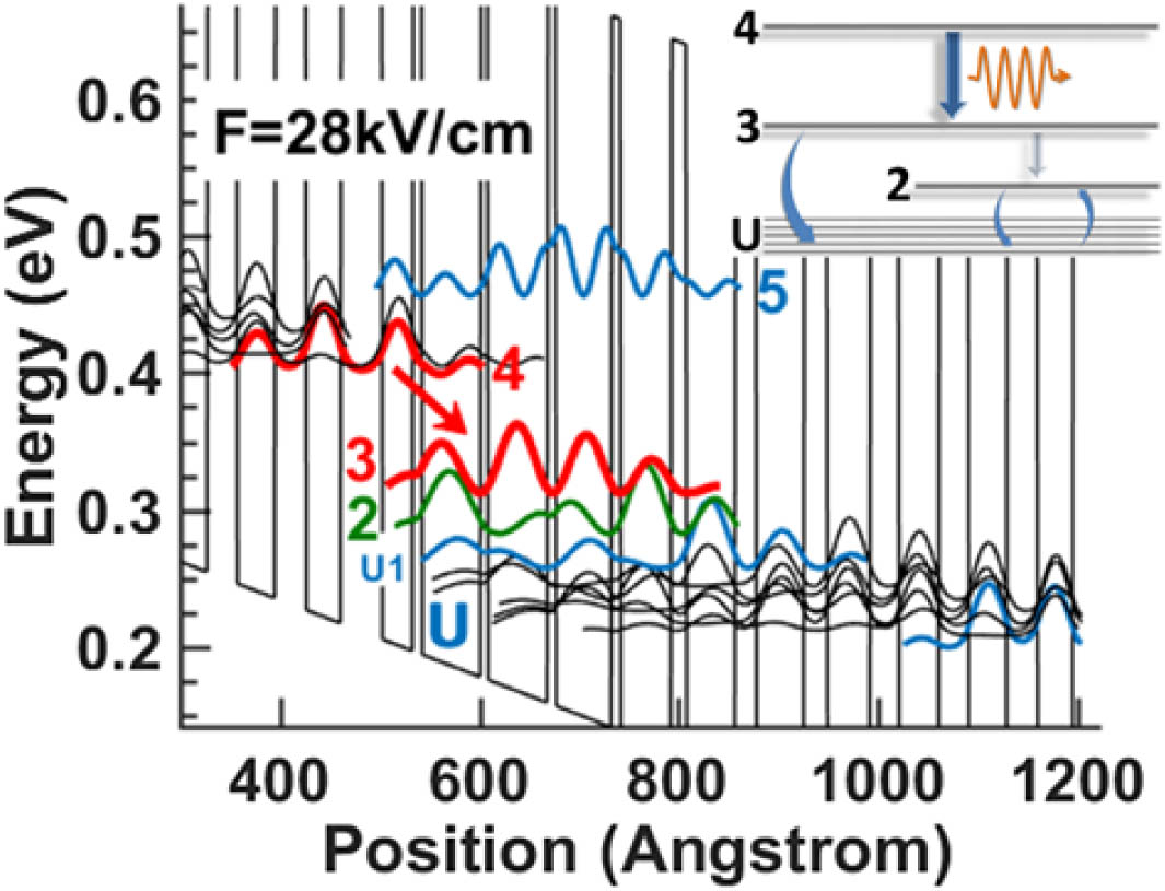
We present a long-wavelength QCL structure design combined with the diagonal optical transition [18] and nonresonant extraction [8] mechanism. In this way, the diagonal transition reduces carrier injection leakage, and the two-phonon resonance condition is removed without sacrificing the efficient carrier extraction from the lower laser level. A schematic conduction band diagram at an applied electric field of 28 kV/cm is shown in Fig. 1. The design emission wavelength at room temperature is 14.2 μm. The main points of the active region design include the following aspects.
Efficient electron injection into the upper laser level is guaranteed. The upper laser level is nonlocalized, and its wave function overlaps strongly with the injector miniband (the width is ). This leads to strong coupling of the injector ground state with the laser upper level, . Electron resonant tunneling takes place from the injector ground state to upper laser level 4. At the same time, phonon-assisted scattering enables direct electron injection from high injector levels. The energy spacing between the upper laser level and the active region level located above it, , is 57.3 meV. It helps keep a lower electron thermal activation leakage into the continuum.
The depopulation of the lower laser level is mainly accomplished by LO-phonon-assisted bound-to-continuum scattering from level 3 to the miniband . The carrier lifetime for an energy level can be written as , where is the scattering time from the energy level to a final level and the summation is over all possible final states. The injector miniband was designed to deeply penetrate into the active region below level 2 and suppress the extension of wave functions to the active region above level 4 in the next period. Due to the availability of multiple parallel transitions in the miniband for electron relaxation from level 3, the calculated electron lifetime is only 0.27 ps.
The bound-to-bound diagonal optical transition between level 4 and 3 is guaranteed. The overlap between the upper laser levels and lower levels is reduced while keeping a high diagonal transition matrix element () for laser transition and large upper laser level lifetime . The designed voltage efficiency in the form of the ratio of the photon energy to the potential energy drop per stage is 41.6% at 300 K.
The thermal backfilling of electrons to the lower laser level is prevented. As reported in this paper, the separation between lower laser level 3 and the ground state of the next injector is 116 meV. The energy separation ( and ) in the active region is less than the LO phonon energy (). It is energetically forbidden in general for electrons to relax by resonant LO phonon scattering from level 3 to 2. At room temperature, the electrons at level 3 can get enough energy through thermal activation to emit LO phonons to level 2, but they need to exchange momentum in order to maintain momentum conservation between the initial and final states. Like electrons scattering from level 3 to the miniband , scattering from level 2 to is also efficient. So energy level 2 approximates an empty state and can effectively shield the injector electrons in thermal backfilling to lower laser level 3. It is the most noticeable feature of this new structure.
Figure 1.Schematic conduction band diagram of a portion of the active layers under an applied electronic field of 28 kV/cm. The moduli squared of the relevant wave functions are shown. The layer sequence of one period of the structure in angstroms starting from the injection barrier (toward the right side) is as follows: 41/31/9/59/7/60/8/56/9/51/15/49/21/48/23/43/29/40/30/38/31/35, where barrier layers are in bold, quantum wells are in roman, and the doped layers (Si, ) are underlined. The inset shows a schematic of the diagonal transition and nonresonant extraction scheme.
The QCL structure was grown on n-doped (Si, ) InP substrate by solid-source molecular beam epitaxy (MBE). The Si doping level in the active region was empirically adjusted to to get a high dynamic range. The complete structure along the growth direction includes a 4 μm thick lower InP cladding layer (Si, ), a 0.3 μm thick n- layer (Si, ), 55 stages of the active/injector region, a 0.3 μm thick layer (Si, ), a 5 μm thick upper cladding layer (Si, ), a 0.15 μm gradually doped layer (Si, from to ), and a 0.8 μm highly doped cladding layer (Si, ). After growth, the epitaxial materials were characterized by double crystal X-ray diffraction (XRD) and transmission electron microscopy (TEM).
The double channel waveguides with a ridge width of 40 μm were fabricated by photolithography and wet chemical etching. Then, a 450 nm thick layer was deposited around the ridges by plasma enhanced chemical vapor deposition (PECVD) for electrical insulation. A 200 nm thick Ti/Au layer was deposited by e-beam evaporation to realize the electrical contact after opening a 20 μm wide window through the insulation layer for current injection. In order to reduce thermal resistance, an additional 5 μm thick Au layer was subsequently electroplated. After substrate thinning and backside alloying, the wafer was cleaved into 4 mm long lasers, and subsequently HR coated for the rear facets. Finally, the chips were mounted with the epilayer side down on the copper heat sink with indium solder for characterization.
3. RESULTS AND DISSCUSSION
The lasing spectra were recorded through a Fourier-transform infrared spectrometer at a resolution of in rapid scan mode. Figure 2 displays the lasing spectra of the laser with 1.1 times threshold current at different heat sink temperatures ranging from 293 to 353 K. The emission wavelength is around 14 μm, which is consistent with the design. The peak wavelengths show a slight redshift with increase of the temperature from 14.0 μm at 293 K to 14.02 μm at 353 K. The inset of Fig. 2 shows the lateral (slow axis) far-field characteristics of the laser operating under an injection current of 7.0 A at 293 K. The far-field pattern shows normal single-lobed distribution, which originates from the fundamental lateral mode emission. The full width at half-maximum (FWHM) of the far-field patterns is 17.95°.
Figure 2.Lasing spectra of the QCL at various temperatures. The inset is a lateral far-field radiation pattern at the heat sink temperature of 293 K.
The optical output power was collected by an air-cooled thermocouple detector. Figure 3 shows the typical power-current-voltage (PIV) characteristics at different heat sink temperatures for an HR-coated 4 mm long and 40 μm wide laser. The device is driven with a 2 μs long current pulse with a repetition rate of 5 kHz. At 293 K, the threshold current density is . The higher doping level in the active region used to achieve a larger dynamic range resulted in a relatively higher threshold current density compared to the similar long-wavelength QCLs [18]. The maximum peak output power reaches 830 mW at the rollover current of 9.4 A. The slope efficiency is 271 mW/A. When the temperature increases to 353 K, the threshold current density increases to , and the peak power is still more than 400 mW. The internal quantum efficiency of the device can be calculated by the following equation: where , , , , , , and represent slope efficiency, photon energy, elemental electronic charge, number of cascade period, mirror loss, waveguide loss, and internal quantum efficiency of each period. By an optical simulation, the calculated effective complex refractive index . The waveguide loss can be calculated as . The mirror loss is calculated with the formula , where is the cavity length, and and are facet reflectivities. According to Eq. (1), the internal quantum efficiency is calculated to 16% per cascade period at 293 K.
Figure 3.Pulsed PIV characteristics for an HR-coated 4 mm long and 40 μm wide QCL at various heat sink temperatures. The frequency of driving current is 5 kHz, and the duration is 2 μs.
Based on the measured PIV data, the threshold current density and slope efficiency of the device as functions of temperature are shown in Fig. 4. The pulsed characteristic temperatures and of the laser device can be fitted with usual exponential function as follows: where th is the threshold current density. The dashed curve is the exponential fit to the threshold current density and the slope efficiency. As a result, the characteristic temperature extracted from this fit turns out to be and . This quite high is one of the best results for QCLs operating at similar wavelengths [13,18]. This indicates that the electron thermal backfilling into lower laser level 3 and thermal activation leakage from upper laser level 4 to much higher continuum states are efficiently suppressed by employing a diagonal transition and nonresonant extraction design.
Figure 4.Threshold current density and slope efficiency at different temperatures, where the dashed curves are theoretical fittings.
The average power under different duty cycle (1%–15%) operation from 293 to 353 K is shown in Fig. 5. The average power reaches a maximum of 75 mW with a duty cycle of 15% at 293 K. At 353 K, the maximum average power is still above 16 mW. To our knowledge, this is the highest average power reported to date for a QCL with an emission wavelength μ, which is 1 order of magnitude higher than ever reported to our knowledge [12,18]. The thermal resistance () of the lasers can be roughly estimated by the following equation [19]: where is the heat sink temperature, is the average current, and is the maximum allowable duty cycle at which the average power goes to zero. Limited by the maximum cooling capacity of the test system, the maximum allowable duty cycle at 293 K cannot be measured. At 353 K, the maximum operating duty cycle of the device is . For the 40 μm wide laser, , , and , a thermal resistance of 6.7 K/W was obtained. It should be mentioned here that further improved performance can be expected if a buried-ridge design is used in the laser fabrication.
Figure 5.Average output power characteristics of the laser at heat sink temperatures from 293 to 353 K.
In conclusion, a high-average-power QCL emitting at 14 μm has been demonstrated based on the diagonal transition and nonresonant extraction active region design. At 293 K, an 830 mW peak power was obtained for a double channel ridge waveguide, HR-coated, 55 period quantum cascade laser. The threshold current density is measured as at a duty cycle of 1%, and the maximum average power is achieved up to 75 mW at a duty cycle of 15%. Over a temperature range from 293 to 353 K, a high characteristic temperature of 395 K was achieved.
Acknowledgment
Acknowledgment. The authors thank Ping Liang and Ying Hu for their help in processing.