• Journal of Semiconductors
  • Vol. 40, Issue 7, 071903 (2019)
Shuliang Ren1、2, Qinghai Tan1、2, and Jun Zhang1、2、3、4
Author Affiliations
  • 1Institute of Semiconductors, Chinese Academy of Sciences, Beijing 100083, China
  • 2Center of Materials Science and Optoelectronics Engineering, University of Chinese Academy of Sciences, Beijing 100049, China
  • 3CAS Center of Excellence in Topological Quantum Computation, University of Chinese Academy of Sciences, Beijing 101408, China
  • 4Beijing Academy of Quantum Information Science, Beijing 100193, China
  • show less
    DOI: 10.1088/1674-4926/40/7/071903 Cite this Article
    Shuliang Ren, Qinghai Tan, Jun Zhang. Review on the quantum emitters in two-dimensional materials[J]. Journal of Semiconductors, 2019, 40(7): 071903 Copy Citation Text show less

    Abstract

    The solid state single photon source is fundamental key device for application of quantum communication, quantum computing, quantum information and quantum precious metrology. After years of searching, researchers have found the single photon emitters in zero-dimensional quantum dots (QDs), one-dimensional nanowires, three-dimensional wide bandgap materials, as well as two-dimensional (2D) materials developed recently. Here we will give a brief review on the single photon emitters in 2D van der Waals materials. We will firstly introduce the quantum emitters from various 2D materials and their characteristics. Then we will introduce the electrically driven quantum light in the transition metal dichalcogenides (TMDs)-based light emitting diode (LED). In addition, we will introduce how to tailor the quantum emitters by nanopillars and strain engineering, the entanglement between chiral phonons (CPs) and single photon in monolayer TMDs. Finally, we will give a perspective on the opportunities and challenges of 2D materials-based quantum light sources.

    1. Introduction

    Different from the classical light source, the single photon emitter (SPE) is a fundamental quantum light resource for many scalable quan­tum technologies includ­ing quantum computing, quantum precision measurement and quantum secure communication. The ideal on-demand SPE emits exactly one photon at a time into a given spatiotemporal mode, and all photons are identical so that if any two are sent through separate arms of a beam-splitter, they produce full interference that is a signature of indistinguish ability. Up to now, researchers have found SPEs in zero-dimensional materials, such as GaAs, InGaAs QDs[1, 2]; one-dimensional materials, such as carbon nanotube, InP nanowires[3, 4]; three-dimensional wide bandgap materials, such as diamond and GaN[57]. However, there are many shortcomings that limit their application, for instance, most of quantum emitters in QDs just work at low temperature[1], the brightness and purity for quantum emitters from color centers in carbon nanotubes is low[4], and the emission wavelengths from color center in diamond are limited[8]. Therefore, it is significant continue to find a better single photon source. The discovery of 2D materials opens a new era to study new physical phenomena and related device application owing to its novel properties[9]. Remarkably, traditional solid-state emitters are typically embedded in three-dimensional materials with high-refractive index, which usually limits the integration ability and the photon extraction efficiency. Whereas, the 2D geometry of a SPEs confined to an atomically thin material can in principle greatly enhance the photon extraction efficiency, potentially allowing for simplified integration with photonic circuits, and could facilitate strong and controllable external perturbations due to the close proximity of the embedded SPEs.

    Recently, the SPEs from defect states have been found in various 2D materials, including TMDs MX2 (WSe2, WS2, MoSe2, and MoS2)[1018], GaSe[19], and hBN[2025]. In particular, the SPEs from hBN is stable at room temperature, and even at higher than 800 K[26]. Meanwhile, many methods have been applied to tune and control the properties of quantum emitters in 2D materials, for instance, the magnetic field applying[27], the nanopillar designing[28, 29], strain engineering[19, 30, 31], and coupling to cavity or array chip[31, 32]. Furthermore, the emerging of quantum emitters in 2D materials also provides a new platform to study the quantum physical, for example, the quantum entanglement between phonon and photon. In addition, these 2D materials are convenient to transfer to other 2D materials (heterostructures) or traditional semiconductor materials, thus the advantages of various materials can be integrated into one combined structure, e.g, the integration of monolayer SPEs with photonic crystals can improve the single photon emission rate. The deterministic engineering of SPE arrays in 2D layer by scanning tunneling microscopy technology or strain controlled nanopillar also show amazing potential for scalable quantum technology applications. Therefore, the quantum emitters in 2D materials are expected to play pivotal potential in quantum photonic devices.

    The previous reviews discussed the advances in mastering SPEs in 2D materials[17, 33]. However, the relevant research fields are developing rapidly. Some latest achievements need to be summarized to give guidance for future development. Here, we will give a brief review on the recent progress of quantum emitters in 2D materials. Firstly, we will introduce the quantum emitters from various 2D materials and their characteristics. Secondly, we will introduce the electrically driven quantum light in the TMDs-based LED. Thirdly, we will introduce how to tailor the quantum emitters by nanopillar and strain engineering, and then introduce the entanglement between chiral phonons and single photon in monolayer WSe2. Finally, we will give discussions on the opportunities and challenges of 2D materials-based quantum light sources.

    2. Quantum emitters from various 2D materials

    In the family of 2D materials, TMDs aroused great interest because of their excellent optical properties[9, 34, 35]. In recent years, they have also been studied as the holder of quantum emitters to generate single photon[17]. Four independent research groups firstly found that the isolated defects in the monolayer WSe2 can emit single photon at cryogenic temperatures[14, 15, 18]. These localized SPEs emit single photons with a narrow-linewidth and are composed of a linearly polarized doublet. Polarization-resolved and magneto-optical studies reveal a large zero-field splitting of ~0.71 meV and an exciton g-factor of ~8.7. They proposed that these SPEs are composed of neutral excitons trapped at anisotropic confining potentials from defects in the monolayer.

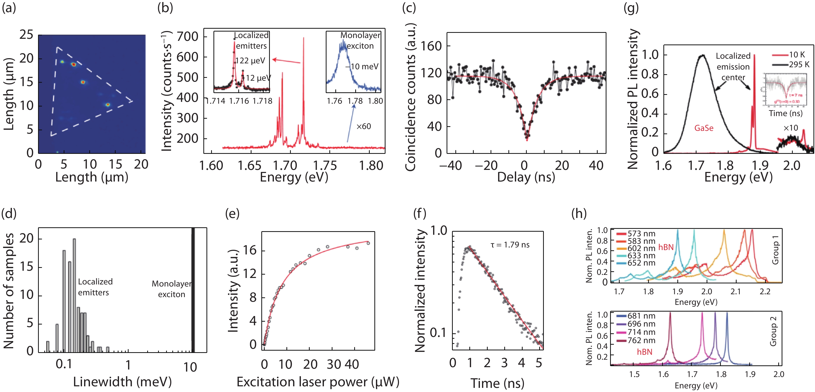
    Fig. 1(a) shows the photoluminescence (PL) intensity mapping of narrow emission lines centered at 1.719 eV in monolayer WSe2, where the triangle indicates the position of the monolayer WSe2. The emissions from defects in WSe2 are expressed by bright spots appeared at three isolated positions, they are different from the emission of intrinsic excitons. Fig. 1(b) shows the PL spectrum of one isolated position in Fig. 1(a), the right inset shows the intrinsic excitons of monolayer WSe2, and the left inset shows one single quantum emitter with doublet peak structure. The narrow linewidth is the most remarkable characteristic of single photon emission in the spectrum. In terms of emission energy, the emission position of defects is red shifted by 40–100 meV from the intrinsic excitons transition of monolayer WSe2, this shows that the energy of the quantum light source is within the bandgap of WSe2. To further confirm the doublet peak is single photon emission, the corresponding second order correlation function was measured, from the fitting data in Fig. 1(c), the means that they are single photon emitters. The number of photons emitted on energy scale can further characterize the single photon emission, a statistical histogram for 92 randomly localized emitters from 15 different monolayers is presented in Fig. 1(d), their spectral linewidths range from 58 to 500 μeV, and their average linewidth is 130 μeV, roughly two orders of magnitude smaller than the linewidth of the delocalized excitons in the PL spectrum. Similar to the atom-like two-level system, integrated intensity of SPEs shows a pronounced saturation behavior when the excitation power exceeds the threshold, as shown in Fig. 1(e). The time-resolved PL shows a single exponential decay with a decay time of [18].

    (Color online) (a) Photoluminescence (PL) intensity map of narrow emission lines centered at 1.719 eV. The dashed triangle indicates the position of the monolayer WSe2[18]. (b) PL spectrum of localized emitters. The left inset is a high resolution spectrum of one SPE. The right inset is an enlarged view of the monolayer excitons emission[18]. (c) Second order correlation measurement of the PL from one SPE in (b)[18]. (d) A histogram comparison of the linewidth between the emission from the delocalized excitons and 92 localized emitters[18]. (e) The integrated counts of the photon emission from SPE as a function of laser power. The red line is a guide to the eye[18]. (f) Time-resolved PL of SPE showing a single exponential with decay time of 1.79 ± 0.002 ns[18]. (g) Typical PL spectra of 36 nm thick GaSe, recorded at a temperature of T = 295 K and T = 10 K, respectively[19]. (h) The PL spectra of single photon emissions from hBN samples[36].

    Figure 1.(Color online) (a) Photoluminescence (PL) intensity map of narrow emission lines centered at 1.719 eV. The dashed triangle indicates the position of the monolayer WSe2[18]. (b) PL spectrum of localized emitters. The left inset is a high resolution spectrum of one SPE. The right inset is an enlarged view of the monolayer excitons emission[18]. (c) Second order correlation measurement of the PL from one SPE in (b)[18]. (d) A histogram comparison of the linewidth between the emission from the delocalized excitons and 92 localized emitters[18]. (e) The integrated counts of the photon emission from SPE as a function of laser power. The red line is a guide to the eye[18]. (f) Time-resolved PL of SPE showing a single exponential with decay time of 1.79 ± 0.002 ns[18]. (g) Typical PL spectra of 36 nm thick GaSe, recorded at a temperature of T = 295 K and T = 10 K, respectively[19]. (h) The PL spectra of single photon emissions from hBN samples[36].

    Quantum emitters based on layered semiconductor GaSe was also reported[19]. The PL emission of GaSe is stable and does not show any blinking or spectral wandering. When there are lattice deformations in the GaSe crystal, the local strain fields from lattice deformation produce a confinement potential for the exciton and form a localized exciton and biexciton. The cascade transition process from biexciton to exciton results in single photon emission. The emitters are from local deformations of the GaSe crystal, which are caused by nanoscale Se clusters[19]. The strain induced in the GaSe crystal leads to local confinement potentials, which trap excitons. Atomic force microscope and energy-dispersive X-ray spectroscopy measurements indicate that the localization of the excitons is related to deformations of the GaSe crystal, caused by incorporated nanoscale selenium clusters. These lattice deformations create local strain fields which induce confinement potentials for the excitons. Power-dependent photoluminescence measurements show that only single-photon emitters exhibit a separate biexciton line in the spectrum. This observation indicates that the spatial extension of the potential wells created by the Se clusters is critical for the formation of the single-photon sources. The strain-induced creation of single-photon emitters provides a route towards the controlled positioning of the light sources on the nanoscale. As shown in Fig. 1(g), the PL exhibits either a single prominent line or a double peak in the range 1.7–2.0 eV, and the second order correlation function for the narrow linewidth luminescence is around 0.33, which further proves that these narrow peaks originate from single photon emissions. The two emission lines from the same emitter are from the localized exciton and biexciton, respectively[19]. The observed biexciton-exciton cascade makes these emitters promising candidates for entangled photon sources.

    The temperature is important for the quantum emitters based devices. 2D material hBN is a promising candidate for new generation single photon sources due to its chemical stability, and large bandgap with about 6 eV of monolayer hBN[37]. In hexagonal boron nitride (hBN), the SPEs have been associated with deep energy level defect states within the large band gap that allow a bright, stable, and broadband SPE at room temperature and even higher temperature. In general, defects are important sources of single photon emissions in hBN, they can be created by annealing and electron beam irradiation. There are broad spectral range of multicolor single photon emissions originated from defects in hBN across the visible and the near-infrared spectral ranges at room temperature[36]. Emitters can be classified into two general groups based on their zero phonon lines (ZPLs) energy and phonon sideband (PSB) spectral shapes. The top part in Fig. 1(h) consists of emitters with ZPL energies at around 576, 583, 602, 633, and 652 nm (Group1). The bottom part in Fig. 1(h) shows these emitters at lower energies, with ZPLs centered on 681, 696, 714, and 762 nm (Group2). Emissions in Group2 have narrower, more symmetric ZPLs, and phonon sidebands are weaker compared to group1. The single photon emissions in hBN can also be extended to the UV region due to its large bandgap[25]. Single photon of hBN in a wide spectral range, lays a good foundation in future, such as applications in nanophotonics and nanoscale sensing devices. The native point defects in hBN are always coupled with phonon states, so the properties of single photon emission in hBN are temperature dependent. Each single photon emission exhibits similar line width broadening and red shifting as temperature increasing, and relative intensity of each single photon emission line decreases exponentially with increasing of temperature[20]. The spin state of single photon emission is important for future quantum information technology. Recently, researcher found the strongly anisotropic photoluminescence patterns as a function of applied magnetic field for select quantum emitters in hBN at room temperature[27], where the spin dependent quantum emission in hBN could be used to initialize or read out spin valley information for other materials.

    3. Electrically driven quantum light in a WSe2-based light-emitting diode

    With the development of technology, nanodevices have been widely used in many fields. In application, most of them are driven by electricity. Electrically driven quantum light source, as the core devices in the field of quantum communication and quantum computing, have attracted more and more attentions[38]. The single photon generation in quantum dots driven by electricity have been widely studied[39]. Three-dimensional material diamond has also been reported to be able to generate single photons by electrical excitation[40]. With the exploration of the optical properties and applications of 2D materials, the emission of single photon from 2D materials driven by electricity has gradually become an attractive subject.

    Recently, Carmen et al. reported the electrically driven quantum light in a WSe2-based LED[41]. Fig. 2(a) gives the illustration of such the device. A heterostructure on a silicon/silicon dioxide (Si/SiO2) substrate consist of a monolayer graphene to be the source of electron injection, a thin sheet hBN which can be used as the tunnel barrier, and a mono- and bilayer WSe2 exfoliated from p-doped bulk crystal which can be used as optically active layers. Metal electrodes provide electrical contact to the graphene and WSe2 layers.

    (Color online) (a) Optical microscope image of a typical device used in experiments. The dotted lines highlight the footprint of the graphene, hBN and the TMD layers individually. The Cr/Au electrodes contact the graphene and TMD layers to provide electrical bias[42]. (b) A raster-scan map of integrated EL intensity from monolayer and bilayer WSe2 areas of the quantum LED for an injection current. The dotted circles highlight the submicron localized emission in this device[42]. (c) A schematic energy band diagram, including the confined electronic states of the QDs. Electro-luminescence(EL) emission from QD starts at lower bias than the conventional LED operation threshold[42]. (d) Typical EL emission spectra for QDs in the monolayer (top) and bilayer (bottom) WSe2. The shaded area highlights the spectral window for LED emission from the bulk WSe2 excitons[42]. (e) Top (bottom) spectra of PL and EL correspond to 10 K (room temperature) operation temperature[42]. (f) Comparison of the integrated EL intensity for the WSe2 layer and for a QD as a function of the applied current. (g) Intensity-correlation function, g(2)(t) of with a rise-time of 9.4 ± 2.8 ns[42].

    Figure 2.(Color online) (a) Optical microscope image of a typical device used in experiments. The dotted lines highlight the footprint of the graphene, hBN and the TMD layers individually. The Cr/Au electrodes contact the graphene and TMD layers to provide electrical bias[42]. (b) A raster-scan map of integrated EL intensity from monolayer and bilayer WSe2 areas of the quantum LED for an injection current. The dotted circles highlight the submicron localized emission in this device[42]. (c) A schematic energy band diagram, including the confined electronic states of the QDs. Electro-luminescence(EL) emission from QD starts at lower bias than the conventional LED operation threshold[42]. (d) Typical EL emission spectra for QDs in the monolayer (top) and bilayer (bottom) WSe2. The shaded area highlights the spectral window for LED emission from the bulk WSe2 excitons[42]. (e) Top (bottom) spectra of PL and EL correspond to 10 K (room temperature) operation temperature[42]. (f) Comparison of the integrated EL intensity for the WSe2 layer and for a QD as a function of the applied current. (g) Intensity-correlation function, g(2)(t) of with a rise-time of 9.4 ± 2.8 ns[42].

    Fig. 2(b) shows the spatial map of integrated Electro-luminescence (EL) from the WSe2-based LED device at 10 K. The spatially uniform light emissions are from delocalized excitons of WSe2. The brighter area corresponds to the bilayer WSe2, suggesting that most of the injected current flows through this region. The dotted circles correspond to highly localized emissions from both the monolayer and the bilayer WSe2. The device is controlled by an applied voltage. At zero bias between the graphene and the monolayer WSe2, the Fermi energy (EF) of the system is the same across the heterostructure. Therefore, this preventing net charge flow (current) between the layers. When a negative bias applied to the graphene electrode, as shown in Fig. 2(c), the graphene EF raises to above the minimum of the conduction band (EC) of grounded WSe2, this induces electrons to tunnel from the graphene into the monolayer WSe2. The radiative recombination between the tunneled electrons and the holes results in the photoemission. When WS2 monolayer exfoliated from an n-doped bulk crystal is integrated into the same device, it can also be electrically driven to emit single photons of different wavelengths[42]. Because the host material influences the quantized energy levels, so the single photon emission wavelength can be adjusted by different 2D materials in electrically driven quantum light device.

    The emissions from TMDs based electrically driven quantum light device also have good quantum qualities. Fig. 2(d) shows the example emissions spectrum from mono- and bilayers WSe2, emission in monolayer and bilayer WSe2 are described by the top and bottom spectrum, respectively. In the spectrum, shaded area highlights the emission due to intrinsic excitons of WSe2, whereas quantum LED (QLED) produces spectra at longer wavelength for both mono- and bilayers of WSe2, because localized states are also within the bandgap of WSe2. In bilayers WSe2, its quantum emission peak is shifted to longer wavelength compared with in monolayer. If different layers of TMDs are integrated into this device, it can be used as a means to adjust the wavelength of single photon emission.

    EL has unique characteristics compared with PL. As shown in Fig. 2(e), when excitons states are excited by electricity at a low-current regime, the localized excitons states respond more efficiently to charge injection than the delocalized ones at 10 K. At room temperature, the emission wavelength of EL shifts to long wavelength due to the charge injection. Fig. 2(f) plots the current dependence of the integrated EL intensity from a quantum emitter, as well as from the unbound monolayer WSe2 excitons. The saturation behavior of QLED intensity with the increase of current intensity is observed. The corresponding second order correlation function of QLED was measured at low temperature, as shown in Fig. 2(g). The 0.5, which can be used as the evidence of single photon emission. This preliminarily proves that it is feasible to control the generation of single photon in 2D materials by the electrical method.

    4. Tailoring the quantum emitters by nanopillars and strain engineering

    2D materials have atomic-level thickness, hence the quantum emitter in 2D material is sensitive to the environment and applied field such as magnetic field, localized plasmonic field as well as strain field. For instance, magnetic fields can dramatically tune the optical spectra of SPEs WSe2 due to its large g factor of ~8.7[18], which is much larger than the single-atom-layer valley excitons and InAs QDs[43]. When the emission of single photon in hBN is coupled with high quality plasmonic nanocavity arrays, the coupled emitters exhibit enhanced emission rates and reduced fluorescence lifetimes, consistent with Purcell enhancement in the weak coupling regime[32]. Besides magnetic field and plasmonic localized enhancement, strain field also provides another choice to modulate the properties of solid SPEs. For instance, strain engineering can create quantum emitters in 2D TMDs materials with precise position, and the emission wavelength and intensity can be easily tuned by changing the strength of strain[28, 30, 44, 45]. When putting the monolayer WSe2 at the nanoscale gap between two single-crystalline gold nanorods, the specific strain landscape leads to the formation of a potential well which can form the quantum emitter[45]. Tailoring the quantum emitters based on monolayer WSe2 and WS2 by nanopillar array is a good choice to create quantum emitters with precise position[28], because the nanopillars can create localized deformations which lead to the quantum confinement of excitons.

    By placing the 2D material on spatially ordered nanopillars, the position of single photon emission can be controlled. A simple method is to create array nanopillars and then covered with monolayer 2D materials[28]. Silica is a convenient material for making nanopillars, and can be fabricated by electron beam lithography, as shown in Fig. 3(a). By using the all-dry viscoelastic transfer technique, the selected WSe2 layered materials (LM) flake are placed onto the patterned nanopillar substrate, as shown in Fig. 3(b). In particularly, when LM is placed on the substrate, it may be pierced by some nanopillars. The dark field optical microscopy image is shown in Fig. 3(c), the regularly spaced bright spots correspond to nanopillar sites, the brighter area which are encircled in pink correspond to locations where the monolayer WSe2 tents over the nanopillars, and fainter intensity area which are encircled in blue latter correspond to locations where the flake is pierced by the nanopillars. Among them, people pay attention to the points that have not been pierced. Most nanopillar sites host single quantum emitters with one emission peak. PL can further give direct evidence that a single photon can be produced at the position of brighter area. The top part of Fig. 3(d) shows the presence of narrow lines at selected nanopillar location. Photon correlation measurements corresponding to the filtered spectral regions with 10 nm enclosed by the blue, green and pink rectangles in spectral are measured, as shown in the bottom part of Fig. 3(d), the corresponding value of is 0.087 ± 0.065, 0.17 ± 0.02 and 0.18 ± 0.03, respectively. The emission characteristics of single photon are dependent on the height of nanopillars. For the taller nanopillars, the linewidth of the emission peaks will be narrower[28]. It is a good method to optimize the quality of single photon by tuning the height of nanopillars. By using the same method, LM can also be replaced by WS2. With the advancement of research, such regular single photon emitters generated through arrays can also be applied to other more 2D materials. In fact, nanopillars can also be replaced by nanodiamonds. It provides an opportunity to create hybrid quantum devices where LM quantum emitters can be coupled to quantum systems in other materials such as spins in diamond and silicon carbide[28].

    (Color online) (a) Scanning electron microscope (SEM) image of nanopillar substrate, fabricated by electron beam lithography[28]. (b) Illustration of the fabrication method: (1) mechanical exfoliation of layered materials (LM) on PDMS and all-dry viscoelastic deposition on patterned substrate; and (2) deposited LM on patterned substrate[28]. (c) Dark field optical microscopy image (real color) of monolayer layer (1L)-WSe2 on nanopillar substrate[28]. (d) PL spectra taken at nanopillar in a low orderly, enclosed by the blue, green and pink rectangles, the Second-order correlation measurement were shown below respectively[28]. (e) Schematic diagram for the strain applied in monolayer (upper part) and bilayer (lower part) geometries[30]. (f) Defect emission lines as a function of pressure, showing a redshift at a rate of 1.31(7) (peak A) and 1.33(3) meV/GPa (peak C) initially as well as a subsequent blueshift at a rate of 0.72(4) (peak B) and 0.67(9) meV/GPa (peak D), respectively, red and blue arrows are guides to the eye[30]. (g) Fitting data of the PL peak energies as a function of pressure[30].

    Figure 3.(Color online) (a) Scanning electron microscope (SEM) image of nanopillar substrate, fabricated by electron beam lithography[28]. (b) Illustration of the fabrication method: (1) mechanical exfoliation of layered materials (LM) on PDMS and all-dry viscoelastic deposition on patterned substrate; and (2) deposited LM on patterned substrate[28]. (c) Dark field optical microscopy image (real color) of monolayer layer (1L)-WSe2 on nanopillar substrate[28]. (d) PL spectra taken at nanopillar in a low orderly, enclosed by the blue, green and pink rectangles, the Second-order correlation measurement were shown below respectively[28]. (e) Schematic diagram for the strain applied in monolayer (upper part) and bilayer (lower part) geometries[30]. (f) Defect emission lines as a function of pressure, showing a redshift at a rate of 1.31(7) (peak A) and 1.33(3) meV/GPa (peak C) initially as well as a subsequent blueshift at a rate of 0.72(4) (peak B) and 0.67(9) meV/GPa (peak D), respectively, red and blue arrows are guides to the eye[30]. (g) Fitting data of the PL peak energies as a function of pressure[30].

    Strain engineering, another strain controlled method for single photon emission in 2D materials, has good application prospects. By using nanoscale elastic strain engineering in WSe2, it can deterministically generate robust quantum emitters by apply local modification of the electronic and optical properties[29]. The advantage of strain engineering for single photon emission is that the wavelength of single photon emission can be adjusted by different stress. When the strain is applied to hBN by hydrostatic pressure technique at the low temperature, as shown in Fig. 3(e), this will change the intralayer and interlayer interaction in hBN flake, thus changing the behavior of single photon emission. These PL emission lines in Fig. 3(f) indicate that different pressures lead to different emission wavelength. The experimental results of the pressure-dependent PL emission lines present three different types of pressure responses corresponding to a redshift (negative pressure coefficient), a blueshift (positive pressure coefficient), or even a sign change from negative to positive as shown in Fig. 3(g). According to the theoretical calculation results of density functional theory, defects NBVN in hBN are the sources of single photon emission. In monolayer hBN, intralayer interaction is dominant and causes a blueshift of emission peak, while for bilayer hBN, the interlayer interaction component is dominant and leads to a redshift of the emission peak[30]. Another group also reported that strain engineering can adjust single photon emission characteristics from defect states NBVN in hBN, where NBVN defects can be obtained by He+ irradiation on an exfoliated 100 nm-thick hBN flake. Transferring the hBN films onto a bendable 1.5 mm-thick polycarbonate (PC) beam can achieve the controlling of strain engineering. Strain control allows spectral tunability of hBN single photon emitters over 6 meV. In this way, the emission intensity of single photon can be achieved 7 × 10⁶ counts per second[44]. It provides a high quality single photon source for future quantum devices.

    5. The entanglement between phonons and single photon

    The strain not only can tune the quantum emission, but also can tune the phonon vibration through lattice deformation. This rises an opportunity to tune the defect-phonon coupling and quantum entanglement between photon and phonon[46]. Detail reports can be found in system of diamond optomechanics[47], where the quantum superposition states can be achieve by coupling the single color center states such as nitrigen vacancy (NV) or silicon vacancy (SiV) with the mechanical phonon or lattice phonon. Such a phonon-photon coupling system shows many interesting quantum phenomena such as quantum ground state cooling[48] and entanglement of phonon-photon[49]. Comparing with diamond, the flexibility and strong electron-phonon coupling of 2D materials offer more possibilities for the realization of quantum optomechanical platforms based on single quantum emitter and phonon. Non-degenerate chiral phonon (CPs) exists in systems where time inversion symmetry or space inversion symmetry is destroyed. When the lattice of crystal has degenerate, low-energy electronic states will be the handedness in the momentum space[50]. There are CPs in honeycomb lattice with angular momentum of along the out-of-plane direction. The chirality-dependent coupling between a single optical excitation and CPs is an important routine to achieve quantum controlling of the emission of single photon as well as quantum entanglement between photon and phonon. Recently, Lu et al. reported the entanglement between CPs and single-photon emitter in of monolayer WSe2[51].

    Fig. 4(a) shows the basic experimental configuration. The monolayer WSe2/hBN stack connected with metal electrodes, which can be regarded as a field effect transistor device. By tuning the voltage, different energy of emission can be obtained from QDs in monolayer WSe2. Fig. 4(b) shows the basic idea behind entanglement of a CP with an photon. In previous studies, CP in WSe2 has been reported[52]. The CPs modes involve a collective excitation of ~109 atoms of the monolayer WSe2. Entanglement arises from angular momentum selection rules of the phonon-scattering process during photon emission, where the polarization of the single photon correlates with the angular momentum of the doubly degenerate CPs. The optical excitations are superposition of left and right circularly polarized states with angular momentum of ±1 along the out-of-plane direction. Due to the conservation of angular momentum in a three-fold symmetric crystal, CPs couple only with circularly polarized states photon, and the photon states involved in the superposition can scatter by two indistinguishable paths with angular momentum conservation correlating the states of their polarization. As a result, after the scattering process, the state of the phonon–photon is , where the ± sign the orthogonal polarization of the incoming photon, labels the helicity of the out-going photon. This state is the maximal entangled state of a phonon–photon system.

    (Color online) (a) Optical image of the monolayer WSe2/hBN stack. The dashed square indicates the scanning area in the PL mapping measurements[51]. (b) Schematic of phonon–photon entanglement. The circularly polarized states () with an angular momentum of 1 = ± 1 are degenerate in WSe2 due to time-reversal symmetry[51]. (c) A PL spectrum at Vg = − 78 V. The splitting energy of the doublets is identical to that of the corresponding b doublets. The energy spacing between a and b doublets is the energy of the (Γ) phonon. Inset shows similar behavior for the QD D6[51]. (d) Polarization of the D3a doublet measured in the linear basis. The lines are fits to the experimental data (dots). (e)The orange dashed line shows an example of the linearly polarized emission in the linear basis measurement, the red dashed circle with a radius of 0.5 can be either circularly polarized emission or an unpolarized light source. The green dashed line shows an example of circularly polarized emission in a circular basis measurement while the red dashed circle with a radius of 0.5 represents unpolarized emission[51].

    Figure 4.(Color online) (a) Optical image of the monolayer WSe2/hBN stack. The dashed square indicates the scanning area in the PL mapping measurements[51]. (b) Schematic of phonon–photon entanglement. The circularly polarized states ( ) with an angular momentum of 1 = ± 1 are degenerate in WSe2 due to time-reversal symmetry[51]. (c) A PL spectrum at Vg = − 78 V. The splitting energy of the doublets is identical to that of the corresponding b doublets. The energy spacing between a and b doublets is the energy of the (Γ) phonon. Inset shows similar behavior for the QD D6[51]. (d) Polarization of the D3a doublet measured in the linear basis. The lines are fits to the experimental data (dots). (e)The orange dashed line shows an example of the linearly polarized emission in the linear basis measurement, the red dashed circle with a radius of 0.5 can be either circularly polarized emission or an unpolarized light source. The green dashed line shows an example of circularly polarized emission in a circular basis measurement while the red dashed circle with a radius of 0.5 represents unpolarized emission[51].

    Fig. 4(c) shows the cross sectional PL spectra at a fixed Vg. The parent emission peaks marked by “a” can be classified some groups according to their energy. The splitting peaks marked by “b” correspond to entanglement process. Moreover, the energy spacing between “a” and “b” peaks, for all the three QDs is precisely 21.8 meV. This energy spacing is exactly equal to the measured energy of the phonon, suggesting the lower-energy “b” peaks are the chiral phonon replica of the parent “a” peaks.

    The polarization properties of the doublets are essential factor to further understand of detail of entanglement. Fig. 4(d) shows that the red and blue peaks of the D3a parent peak are linearly polarized and orthogonal to each other. This is consistent with the D3a doublet’s assignment as a localized X0. However, the b peaks, in spite of being phonon replicas and inheriting all their properties from the parent peaks, show completely unpolarized emission in both linear and circular basis measurements as shown in Fig. 4(e). Considering the mixed state of polarization, , it means that the state is independent of the choice of basis function. It also agrees with the experimental results. Even though there is no measurement of phonon angular momentum in the experiment, it lays the groundwork for the realization of quantum controlling single photon emission in 2D materials[52].

    6. Conclusion and outlook

    As the holders of quantum emitters, 2D materials have great advantages, one of which is that the extraction efficiency of luminescence can reach near unity because it is no longer reflected back to materials due to the atomic thickness. TMDs, as an important member of 2D material family, have good optical properties, and show great potential as quantum emitters in many studies. But their bandgap determines that in most cases they can only emit stable and distinguishable single photons at low temperatures. As another 2D material with wide bandgap, hBN can overcome the problem that single photon cannot be emitted at room temperature, even at higher temperature. Together with tunable emission wavelength and high brightness, hBN will be one of best candidate for room temperature single photon source. However, there is still much challenge to prepare mono- and few-layer 2D materials samples with large area and high quality. Mechanical exfoliation method can obtain 2D materials with good quality, but the size is small and the yield is low. Chemical vapor deposition can be used to synthesize many 2D materials, but it often has high requirements for substrates. At the same time, in the process of material synthesis by chemical method, the quality is usually not good enough. Therefore, it is necessary to make defects controllable in 2D materials for improving the performance of single photon devices. Recently, Liu’s group in Peaking University reported epitaxial growth of a 100-square-centimetre single-crystal hexagonal boron nitride monolayer on copper substrate[53]. This fantastic technique provides a good solution to scale up the 2D quantum emitters.

    2D Van der Waals heterostructure assembled by different 2D materials can also be easily coupled with other devices such as photonic crystal and plasmonic nanocavity. It provides many opportunities to tune the properties of quantum emitters. In particular, by tuning the angle between bilayer TMDs heterostructures, the interlayer Moiré exciton can be generated at certain twist angle owing to the exciton trapped by Moiré periodic potential[54]. The angle sensitive Moiré excitons are good potential for single photon source. Because the stacking order of the heterostructure has a great influence on band alignment, it requires more precise methods to fabricate the required heterostructure. At present, there are still many challenges to be solved. In addition, electric driven and on-chip single photon sources in 2D heterostructure also are very important direction, but the unstable emission of single photon caused by circuit noise still needs to be solved.

    The physical origin of single photon emission is unclear up to date. Once the origin of defect sates in 2D materials is known, the single photon emitter or SPE array could be easily produced on demand by ion implanting or chemical doping. By coupling 2D materials on the nanopillars, it is easy to generate quantum emitter array by strain effects, but uniformity and stability of different emitter pixel need to be improved for quantum application. The quantum entanglement between single photon and chiral phonon opens up the feasibility of controlling single photon emission by phonons. This also provides a good foundation for the development of quantum optomechanical devices in 2D materials.

    Acknowledgments

    We acknowledge support from the National Basic Research Program of China (Grant No. 2017YFA0303401, 2016YFA0301200), Beijing Natural Science Foundation (JQ18014), and Strategic Priority Research Program of Chinese Academy of Sciences (Grant No. XDB28000000).

    References

    [1] J Hours, S Varoutsis, M Gallart et al. Single photon emission from individual GaAs quantum dots. Appl Phys Lett, 82, 2206(2003).

    [2] E Stock, T Warming, I Ostapenko et al. Single-photon emission from InGaAs quantum dots grown on (111) GaAs. Appl Phys Lett, 96, 145(2010).

    [3] D Dalacu, P J Poole, R L Williams. Nanowire-based sources of non-classical light. Nanotechnology, 30, 232001(2019).

    [4] X Ma, N F Hartmann, J K Baldwin et al. Room-temperature single-photon generation from solitary dopants of carbon nanotubes. Nate Nanotechnol, 10, 671(2015).

    [5] M Arita, F Le Roux, M J Holmes et al. Ultraclean single photon emission from a GaN quantum dot. Nano Lett, 17, 2902(2017).

    [6] I Aharonovich, E Neu. Diamond nanophotonics. Adv Opt Mater, 2, 911(2014).

    [7] N Elke, H Christian, H Michael et al. Low-temperature investigations of single silicon vacancy colour centres in diamond. New J Phys, 15, 043005(2013).

    [8] I Aharonovich, C Zhou, A Stacey et al. Enhanced single-photon emission in the near infrared from a diamond color center. Phys Rev B, 79, 1377(2009).

    [9] S Manzeli, D Ovchinnikov, D Pasquier et al. 2D transition metal dichalcogenides. Nat Rev Mater, 2, 17033(2017).

    [10] A Srivastava, M Sidler, A V Allain et al. Optically active quantum dots in monolayer WSe2. Nat Nanotechnol, 10, 491(2015).

    [11] C Chakraborty, K M Goodfellow, V A Nick. Localized emission from defects in MoSe2 layers. Opt Mater Express, 6, 2081(2016).

    [12] C Cong, J Shang, Y Wang, T Yu. Optical properties of 2D semiconductor WS2. Adv Opt Mater, 6, 1700767(2018).

    [13] H M Hill, A F Rigosi, C Roquelet et al. Observation of excitonic rydberg states in monolayer MoS2 and WS2 by photoluminescence excitation spectroscopy. Nano Lett, 15, 2992(2015).

    [14] M Koperski, K Nogajewski, A Arora et al. Single photon emitters in exfoliated WSe2 structures. Nat Nanotechnol, 10, 503(2015).

    [15] C Chakraborty, L Kinnischtzke, K M Goodfellow et al. Voltage-controlled quantum light from an atomically thin semiconductor. Nat Nanotechnol, 10, 507(2015).

    [16] Y Ye, X Dou, K Ding et al. Single photon emission from deep-level defects in monolayer WSe2. Phys Rev B, 95, 245313(2017).

    [17] J D Qiao, F H Mei, Y Ye. Single-photon emitters in van der Waals materials. Chin Opt Lett, 17, 020011(2019).

    [18] Y M He, G Clark, J R Schaibley et al. Single quantum emitters in monolayer semiconductors. Nat Nanotechnol, 10, 497(2015).

    [19] P Tonndorf, S Schwarz, J Kern et al. Single-photon emitters in GaSe. 2D Mater, 4, 021010(2017).

    [20] N R Jungwirth, B Calderon, Y Ji et al. Temperature dependence of wavelength selectable zero-phonon emission from single defects in hexagonal boron nitride. Nano Lett, 16, 6052(2016).

    [21] T T Tran, C Zachreson, A M Berhane et al. Quantum emission from defects in single-crystalline hexagonal boron nitride. Phys Rev Appl, 5, 034005(2016).

    [22] B Sontheimer, M Braun, N Nikolay et al. Photodynamics of quantum emitters in hexagonal boron nitride revealed by low-temperature spectroscopy. Phys Rev B, 96, 121202(2017).

    [23] Z Shotan, H Jayakumar, C R Considine et al. Photoinduced modification of single-photon emitters in hexagonal boron nitride. ACS Photonics, 3, 2490(2016).

    [24] A W Schell, T T Tran, H Takashima et al. Non-linear excitation of quantum emitters in hexagonal boron nitride multiplayers. APL Photonics, 1, 091302(2016).

    [25] R Bourrellier, S Meuret, A Tararan et al. Bright UV single photon emission at point defects in h-BN. Nano Lett, 16, 4317(2016).

    [26] M Kianinia, B Regan, S A Tawfik et al. Robust solid-state quantum system operating at 800 K. ACS Photonics, 4, 768(2017).

    [27] A L Exarhos, D A Hopper, R N Patel et al. Magnetic-field-dependent quantum emission in hexagonal boron nitride at room temperature. Nat Commun, 10, 222(2019).

    [28] C Palacios-Berraquero, D M Kara, A R P Montblanch et al. Large-scale quantum-emitter arrays in atomically thin semiconductors. Nat Commun, 8, 15093(2017).

    [29] A Branny, S Kumar, R Proux et al. Deterministic strain-induced arrays of quantum emitters in a two-dimensional semiconductor. Nat Commun, 8, 15053(2017).

    [30] Y Xue, H Wang, Q Tan et al. Anomalous pressure characteristics of defects in hexagonal boron nitride flakes. ACS Nano, 12, 7127(2018).

    [31] J E Kennard, J P Hadden, L Marseglia et al. On-chip manipulation of single photons from a diamond defect. Phys Rev Lett, 111, 213603(2013).

    [32] T T Tran, D Wang, Z Q Xu et al. Deterministic coupling of quantum emitters in 2D materials to plasmonic nanocavity arrays. Nano Lett, 17, 2634(2017).

    [33] I Aharonovich, D Englund, M Toth. Solid-state single-photon emitters. Nat Photonics, 10, 631(2016).

    [34] F Xia, H Wang, D Xiao et al. Two-dimensional material nanophotonics. Nat Photonics, 8, 899(2014).

    [35] R Lv, J A Robinson, R E Schaak et al. Transition metal dichalcogenides and beyond: synthesis, properties, and applications of single- and few-layer nanosheets. Accounts Chem Res, 48, 56(2015).

    [36] T T Tran, C Elbadawi, D Totonjian et al. Robust multicolor single photon emission from point defects in hexagonal boron nitride. ACS Nano, 10, 7331(2016).

    [37] K Watanabe, T Taniguchi, H Kanda. Direct-bandgap properties and evidence for ultraviolet lasing of hexagonal boron nitride single crystal. Nat Mater, 3, 404(2004).

    [38] Q H Wang, K Kalantar-Zadeh, A Kis et al. Electronics and optoelectronics of two-dimensional transition metal dichalcogenides. Nat Nanotechnol, 7, 699(2012).

    [39] Z Yuan, B E Kardynal, R M Stevenson et al. Electrically driven single-photon source. Science, 295, 102(2002).

    [40] .

    [41] S Schwarz, A Kozikov, F Withers et al. Electrically pumped single-defect light emitters in WSe2. 2D Mater, 3, 025038(2016).

    [42] C Palacios-Berraquero, M Barbone, D M Kara et al. Atomically thin quantum light-emitting diodes. Nat Commun, 7, 12978(2016).

    [43] I Hapke-Wurst, U Zeitler, R J Haug et al. Mapping the g factor anisotropy of InAs self-assembled quantum dots. Physica E, 12, 802(2002).

    [44] G Grosso, H Moon, B Lienhard et al. Tunable and high-purity room temperature single-photon emission from atomic defects in hexagonal boron nitride. Nat Commun, 8, 705(2017).

    [45] J Kern, I Niehues, P Tonndorf et al. Nanoscale positioning of single-photon emitters in atomically Thin WSe2. Adv Mater, 28, 7101(2016).

    [46] M Aspelmeyer, T J Kippenberg, F Marquardt. Cavity optomechanics. Rev Mod Phys, 86, 1391(2014).

    [47] M J Burek, J D Cohen, S M Meenehan et al. Diamond optomechanical crystals. Optica, 3, 1404(2016).

    [48] K V Kepesidis, S D Bennett, S Portolan et al. Phonon cooling and lasing with nitrogen-vacancy centers in diamond. Phys Rev B, 88, 064105(2013).

    [49] E Togan, Y Chu, A S Trifonov et al. Quantum entanglement between an optical photon and a solid-state spin qubit. Nature, 466, 730(2010).

    [50] X Xu, W Yao, D Xiao et al. Spin and pseudospins in layered transition metal dichalcogenides. Nat Phys, 10, 343(2014).

    [51] X Chen, X Lu, S Dubey et al. Entanglement of single-photons and chiral phonons in atomically thin WSe2. Nat Phys, 15, 221(2018).

    [52] H Y Zhu, J Yi, M Y Li et al. Observation of chiral phonons. Science, 359, 579(2018).

    [53] L Wang, X Xu, L Zhang et al. Epitaxial growth of a 100-square-centimetre single-crystal hexagonal boron nitride monolayer on copper. Nature, 570, 91(2019).

    [54] K Tran, G Moody, F Wu et al. Evidence for moire excitons in van der Waals heterostructures. Nature, 567, 71(2019).

    Shuliang Ren, Qinghai Tan, Jun Zhang. Review on the quantum emitters in two-dimensional materials[J]. Journal of Semiconductors, 2019, 40(7): 071903
    Download Citation